Etching solution for removal of oxide film, method for preparing the same, and method of fabricating semiconductor device

Inactive Publication Date: 2006-08-17
SAMSUNG ELECTRONICS CO LTD
View PDF3 Cites 19 Cited by
  • Summary
  • Abstract
  • Description
  • Claims
  • Application Information

AI Technical Summary

Benefits of technology

[0027] The etching solution according to the present invention can remove an oxide film with high etching selectivity while minimizing the loss of a silicon nitride film or a polysilicon film. Furthermore, the etching solution according to the pr

Problems solved by technology

However, the time required to etch oxide films using BOE is long, which increases an etch time loss, thereby leads to cost increase and productivity reduction.
In this respect, for example, when an oxide film that is exposed together with a nitride film or a polysilicon film is etched using BOE or DHF, loss of the nitride film or the polysilicon film when it is exposed together with the oxide film increases, which lowers the efficiency of etching in the oxide film.
After an elevated cylindrical lower electrode is formed, removing the mold oxide film by wet etching using a conventional etching solution may cause serious problems.
In more detail, during the drying process after the mold oxide film has been removed by wet etching, “leaning” phenomenon may occur in which the capacitor lower electrodes are attached to each other due to a tilt by the surface tension of water present between the lower electrodes, thereby causing a 2-bit f

Method used


Image

  • Etching solution for removal of oxide film, method for preparing the same, and method of fabricating semiconductor device
  • Etching solution for removal of oxide film, method for preparing the same, and method of fabricating semiconductor device
  • Etching solution for removal of oxide film, method for preparing the same, and method of fabricating semiconductor device

Examples


experimental example 1

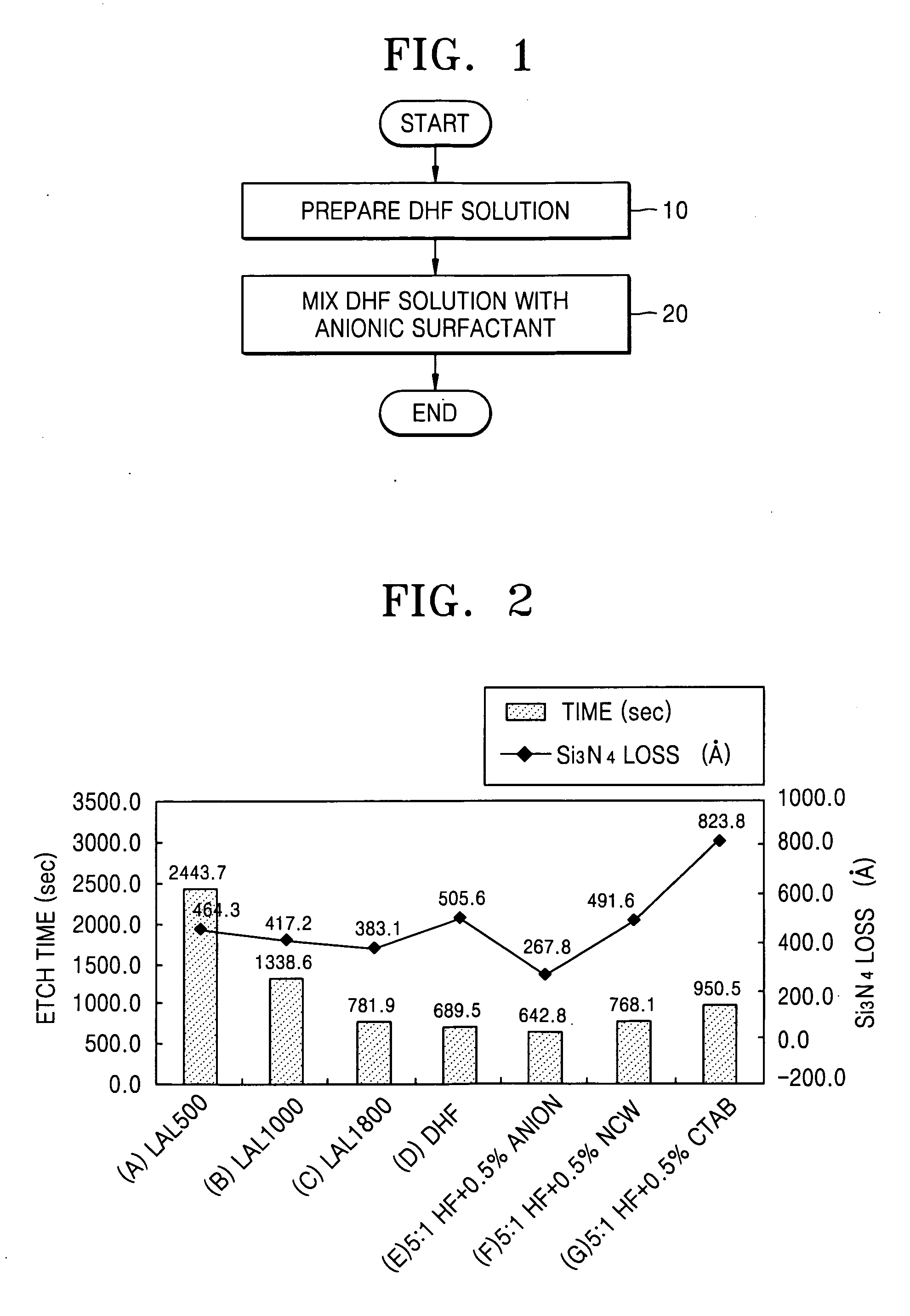
[0048] 0.5 wt % of ammonium lauryl sulfate (ALS) (based on the total weight of an etching solution) used as an anionic surfactant was added to a DHF solution obtained by mixing deionized water and a 50% HF solution in a 5:1 volume ratio to prepare the etching solution.

[0049] A borophosphosilicate glass (BPSG) film (9,000 Å) and a plasma-enhanced tetraethylorthosilicate glass (PE-TEOS) film (16,000 Å) were sequentially deposited on a wafer to form an oxide film with a total thickness of 25,000 Å. While the oxide film was etched using the etching solution at room temperature (25° C.), a silicon nitride (Si3N4) film was simultaneously etched using the same etching solution to measure the loss of the silicon nitride film.

[0050] Measurement results for the etch time of the oxide film and the loss of the silicon nitride film are shown in FIG. 2. In FIG. 2, “(E) 5:1 HF+0.5% anion” represents an etching experiment using the etching solution prepared in Experimental Example 1.

[0051]FIG. 2...

experimental example 2

[0054] 0.1 wt % of ALS (based on the total weight of an etching solution) used as an anionic surfactant was added to a DHF solution obtained by mixing deionized water and a 50% HF solution in a 5:1 volume ratio to prepare the etching solution.

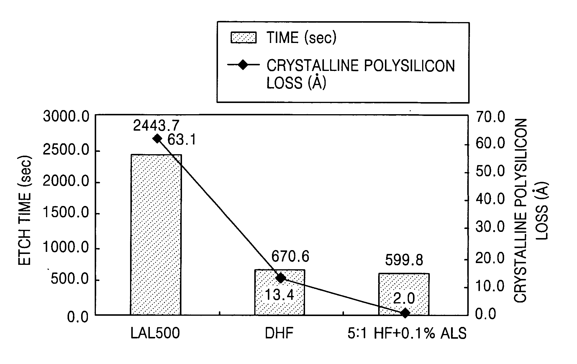
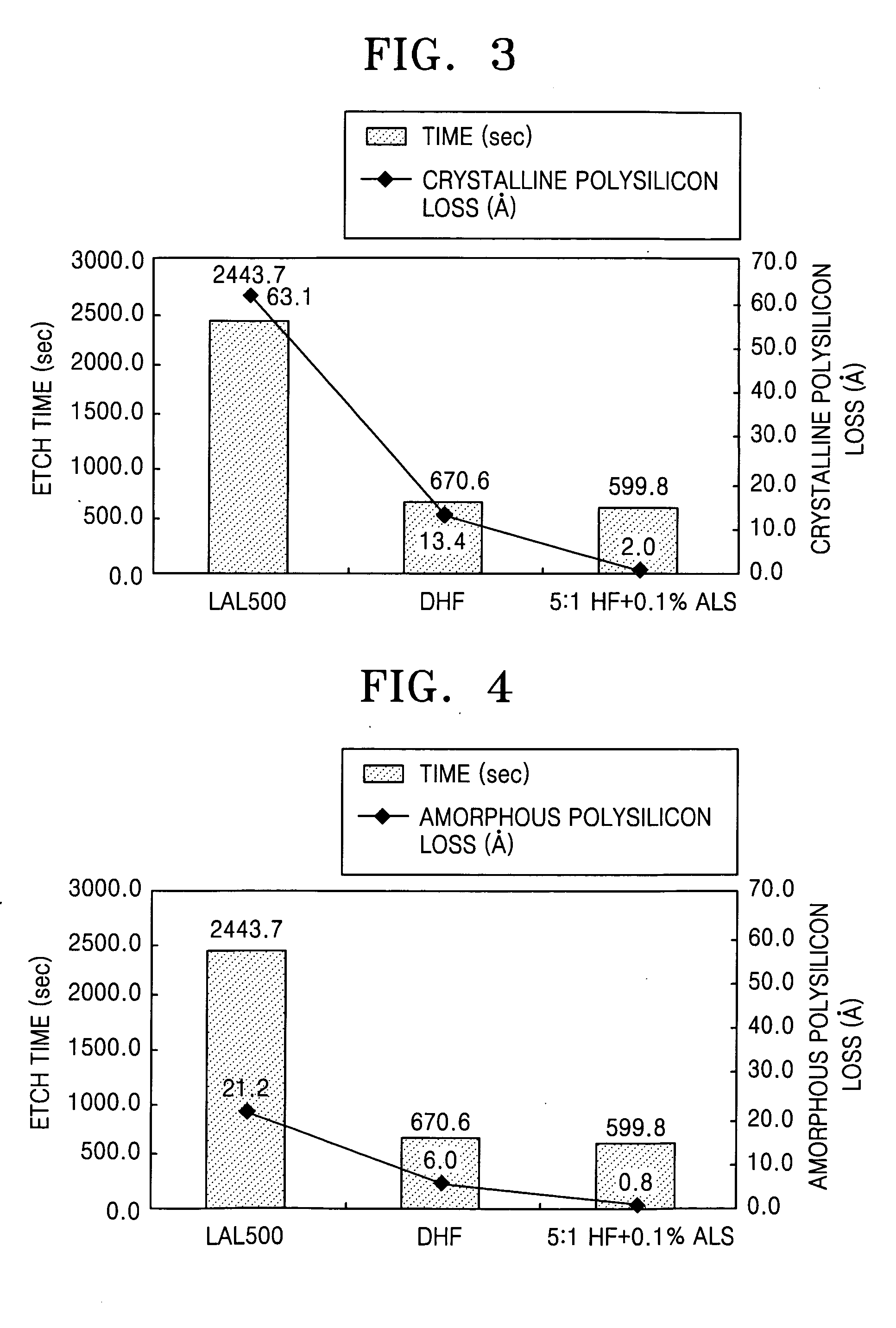
[0055] A BPSG film (9,000 Å) and a PE-TEOS film (16,000 Å) were sequentially deposited on a wafer to form an oxide film with a total thickness of 25,000 Å. While the oxide film was etched using the etching solution at room temperature (25° C.), a crystalline polysilicon film was simultaneously etched using the same etching solution to measure the loss of the crystalline polysilicon film. Here, the crystalline polysilicon film was obtained by forming an amorphous polysilicon film followed by annealing at 850° C. for 30 minutes.

[0056] Measurement results for the etch time of the oxide film and the loss of the crystalline polysilicon film are shown in FIG. 3. In FIG. 3, “5:1 HF+0.1% ALS” represents an etching experiment using the etching solutio...

experimental example 3

[0059] This Experimental Example was performed in the same manner as in Experimental Example 2 except that an amorphous polysilicon film was used instead of the crystalline polysilicon film and the results are shown in FIG. 4. The amorphous polysilicon film was obtained in the same manner as that used in Experimental Example 2 and annealing of the amorphous polysilicon film was omitted.

[0060]FIG. 4 also shows the etching experiment results for the oxide film and the amorphous polysilicon film using surfactant-free etching solutions as controls, i.e., LAL500 and DHF (deionized water:50% HF=5:1).

[0061] As seen from FIG. 4, when the oxide film and the amorphous polysilicon film were simultaneously etched using the etching solution containing ALS as the anionic surfactant according to the present invention, similar results to in FIG. 3 that shows the experimental results for the crystalline polysilicon film were obtained. That is, the etching solution containing ALS used as the anioni...


PUM

PropertyMeasurementUnit
Temperatureaaaaaaaaaa
Fractionaaaaaaaaaa
Weightaaaaaaaaaa

Abstract

Provided are an anionic surfactant-containing etching solution for removal of an oxide film, preparation methods thereof, and methods of fabricating a semiconductor device using the etching solution. The etching solution includes a hydrofluoric acid (HF), deionized water, and an anionic surfactant. The anionic surfactant is a compound in which an anime salt is added as a counter ion, as represented by R1—OSO3HA+, R1—CO2HA+, R1—PO42−(HA+)2, (R1)2—PO4HA+, or R1—SO3HA+ where R1 is a straight or branched hydrocarbon group of C4 to C22 and A is ammonia or amine. The etching solution provides a high etching selectivity ratio of an oxide film to a nitride film or a polysilicon film. Therefore, in a semiconductor device fabrication process such as a STI device isolation process or a capacitor formation process, when an oxide film is exposed together with a nitride film or a polysilicon film, the etching solution can be efficiently used in selectively removing only the oxide film.

Description

CROSS-REFERENCE TO RELATED APPLICATION [0001] This application claims priority under 35 U.S.C. §119 to from Korean Patent Application No. 2004-34566, filed on May 15, 2004, in the Korean Intellectual Property Office, the disclosure of which is incorporated by reference herein in its entirety. BACKGROUND OF THE DISCLOSURE [0002] 1. Field of the Invention [0003] The present invention relates to semiconductor device fabrication. More particularly, the present invention relates to etching solutions for removal of an oxide film, methods for preparing the same, and methods of fabricating a semiconductor device using the etching solution. [0004] 2. Description of the Related Art [0005] Semiconductor device fabrication involves a series of processes including deposition, photolithography, etching, ion implantation, and the like. By these processes, various films such as oxide films, nitride films, polysilicon films, and metal films are formed on a wafer. Patterning these films completes the...

Claims


Application Information

Patent Timeline
IPC IPC(8): H01L21/30H01L21/302H01L21/46C09K13/08C23F1/16H01L21/308H01L21/311H01L21/76H01L21/762H01L21/8242H01L27/108
CPCH01L21/31111H01L21/76224H01L28/40C09K13/08C11D1/02C11D11/0047
Inventor MUN, CHANG-SUPKO, HYUNG-HOSHIM, WOO-GWANHONG, CHANG-KICHOI, SANG-JUN
Owner SAMSUNG ELECTRONICS CO LTD
Why Eureka
Try Eureka