Method and system for providing virtual semiconductor product replicating real semiconductor product

a virtual semiconductor and product technology, applied in semiconductor/solid-state device testing/measurement, instrumentation, design optimisation/simulation, etc., can solve the problems of abandoning the final manufacturing of the intermediate product, unable to perform a process for a more exact unable to achieve a more precise examination of an intermediate product, so as to reduce time and expense, not cause a delay in production

Active Publication Date: 2018-12-13
SK
View PDF7 Cites 2 Cited by
  • Summary
  • Abstract
  • Description
  • Claims
  • Application Information

AI Technical Summary

Benefits of technology

[0005]To address the above-discussed deficiencies of the prior art, it is a primary aspect of the present disclosure to provide a method and a system for providing a virtual semiconductor product replicating a real semiconductor product, which can minimize time and expense required to perform measurement / examination, do not cause a delay in production, and enables processes for an examination and a test.
[0016]According to exemplary embodiments of the present disclosure as described above, the virtual semiconductor product replicating the real semiconductor product is provided in real time with real processing steps, such that time and expense required to measure and examine a semiconductor product can be minimized and a delay in producing semiconductor products is not caused.
[0017]In addition, according to embodiments of the present disclosure, since not only the exterior of the semiconductor product but also the inner structure thereof can be freely observed in three dimensions, the number of times of complicated examinations can be reduced.
[0018]Furthermore, according to embodiments of the present disclosure, since a process for an examination and a test (for example, cutting) can be virtually performed, a more exact examination or assumed test for an intermediate product is enabled without abandoning final manufacturing of the intermediate product, and thus a yield can be improved.

Problems solved by technology

However, measurement / examination requires long time and high expense and may cause a delay in production.
In addition, in measuring and examining using SEM / TEM, it is impossible to perform a process for a more exact examination on an intermediate product (for example, cutting) or a process for a yield improvement test.
This is because the process for this results in abandonment of final manufacturing of the intermediate product.

Method used


Image

  • Method and system for providing virtual semiconductor product replicating real semiconductor product
  • Method and system for providing virtual semiconductor product replicating real semiconductor product
  • Method and system for providing virtual semiconductor product replicating real semiconductor product

Examples


Embodiment Construction

[0026]Hereinafter, the present disclosure will be described in detail with reference to the accompanying drawings.

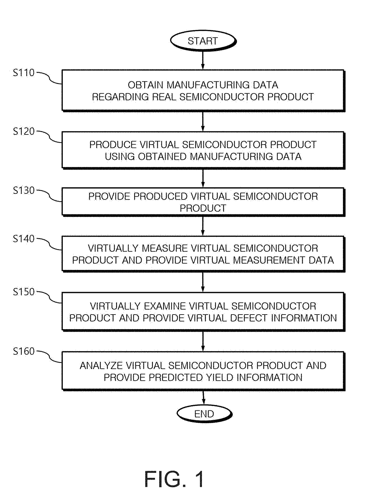
[0027]FIG. 1 is a flowchart provided to explain a method for providing a virtual semiconductor product according to an exemplary embodiment of the present disclosure. The method for providing a virtual semiconductor product according to an exemplary embodiment generates and provides a virtual semiconductor product replicating a real semiconductor product.

[0028]The method illustrated in FIG. 1 may be performed by a “virtual semiconductor product generation system,” which is a kind of a computing system, and more specifically, may be performed by a “virtual semiconductor generation tool,” which is a simulation tool executed in the virtual semiconductor product generation system to virtually produce a semiconductor product.

[0029]As shown in FIG. 1, the virtual semiconductor product generation system obtains data used for manufacturing a real semiconductor, first (S110). The...


PUM


Abstract

A method and a system for providing a virtual semiconductor product replicating a real semiconductor product are provided. The method for providing the virtual semiconductor product according to an exemplary embodiment of the present disclosure includes: obtaining data which is used for manufacturing a real semiconductor; virtually producing a semiconductor product using the obtained manufacturing data; and providing the virtually produced virtual semiconductor product. Accordingly, the virtual semiconductor product replicating the real semiconductor product is provided in real time with real processing steps, such that time and expense required to measure and examine a semiconductor product can be minimized and a delay in producing semiconductor products is not caused.

Description

CROSS-REFERENCE TO RELATED APPLICATION(S) AND CLAIM OF PRIORITY[0001]The present application claims the benefit under 35 U.S.C. § 119(a) to a Korean patent application filed in the Korean Intellectual Property Office on Jun. 12, 2017, and assigned Serial No. 10-2017-0073022, the entire disclosure of which is hereby incorporated by reference.TECHNICAL FIELD OF THE INVENTION[0002]The present disclosure relates generally to semiconductor manufacturing technology, and more particularly, to a method and a system for monitoring a semiconductor manufacturing process in order to detect a defect and predict a yield.BACKGROUND OF THE INVENTION[0003]Measurement performed to detect a defect and predict a yield during a semiconductor manufacturing process may be performed using scanning electron microscope (SEM), transmission electron microscope (TEM), or the like. However, measurement / examination requires long time and high expense and may cause a delay in production.[0004]In addition, in measu...

Claims


Application Information

Patent Timeline
Patent Type & Authority Applications(United States)
IPC IPC(8): G06F17/50
CPCG06F17/5009G06F17/5081H01L22/12H01L22/14H01L22/20H01L22/30G06F30/20G06F30/398
Inventor KIM, SO DAMMOON, YONG SIK
Owner SK
Why Eureka
Try Eureka