Light-emitting element and display device having the light-emitting element

Inactive Publication Date: 2019-01-03
JAPAN DISPLAY INC
View PDF0 Cites 2 Cited by
  • Summary
  • Abstract
  • Description
  • Claims
  • Application Information

AI Technical Summary

Benefits of technology

[0006]An object of an embodiment according to the present invention is to provide a light-emitting element with small variation in property in which properties of the light-emitting element are

Problems solved by technology

Therefore, a micro-resonator is formed in a light-emitting

Method used


Image

  • Light-emitting element and display device having the light-emitting element
  • Light-emitting element and display device having the light-emitting element
  • Light-emitting element and display device having the light-emitting element

Examples


first embodiment

[0029]In the present embodiment, an explanation is made focusing on a structure of a light-emitting element included in a display device 100 according to an embodiment.

1. Outline Structure

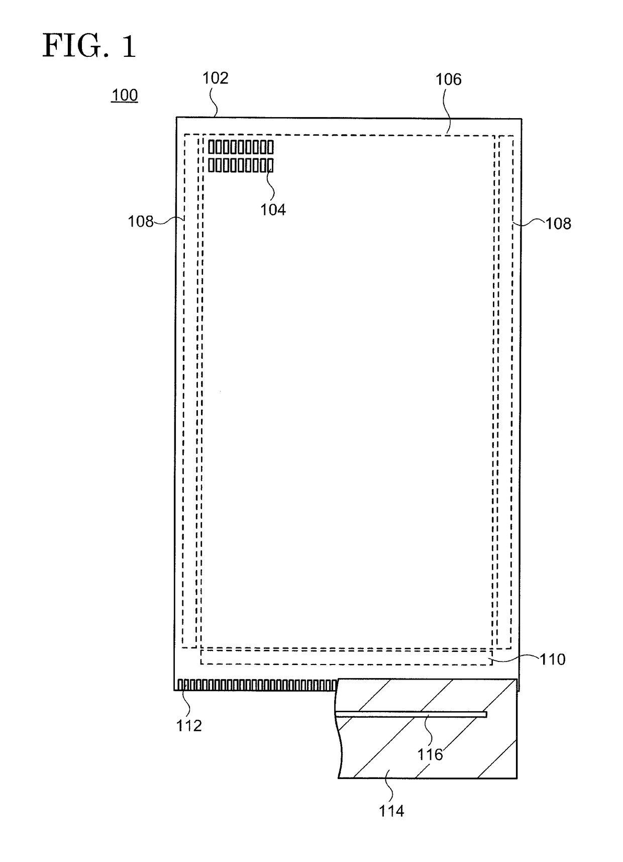
[0030]A schematic top view of the display device 100 is shown in FIG. 1. The display device 100 has a substrate 102 over which a plurality of pixel groups 104 is formed. A display region 106 is defined by the plurality of pixel groups 104, and driver circuits for driving the pixel groups 104 are provided in a region (peripheral region) surrounding the display region 106. In the example shown in FIG. 1, two gate-side driver circuits 108 sandwiching the display region 106, and a source-side driver circuit 110 including analogue switches and the like are disposed. Wirings which are not illustrated extend from the display region 106, the gate-side driver circuits 108, and the source-side driver circuit 110 to a side of the substrate 102 and are exposed at an edge portion of the substrate 102 to form te...

second embodiment

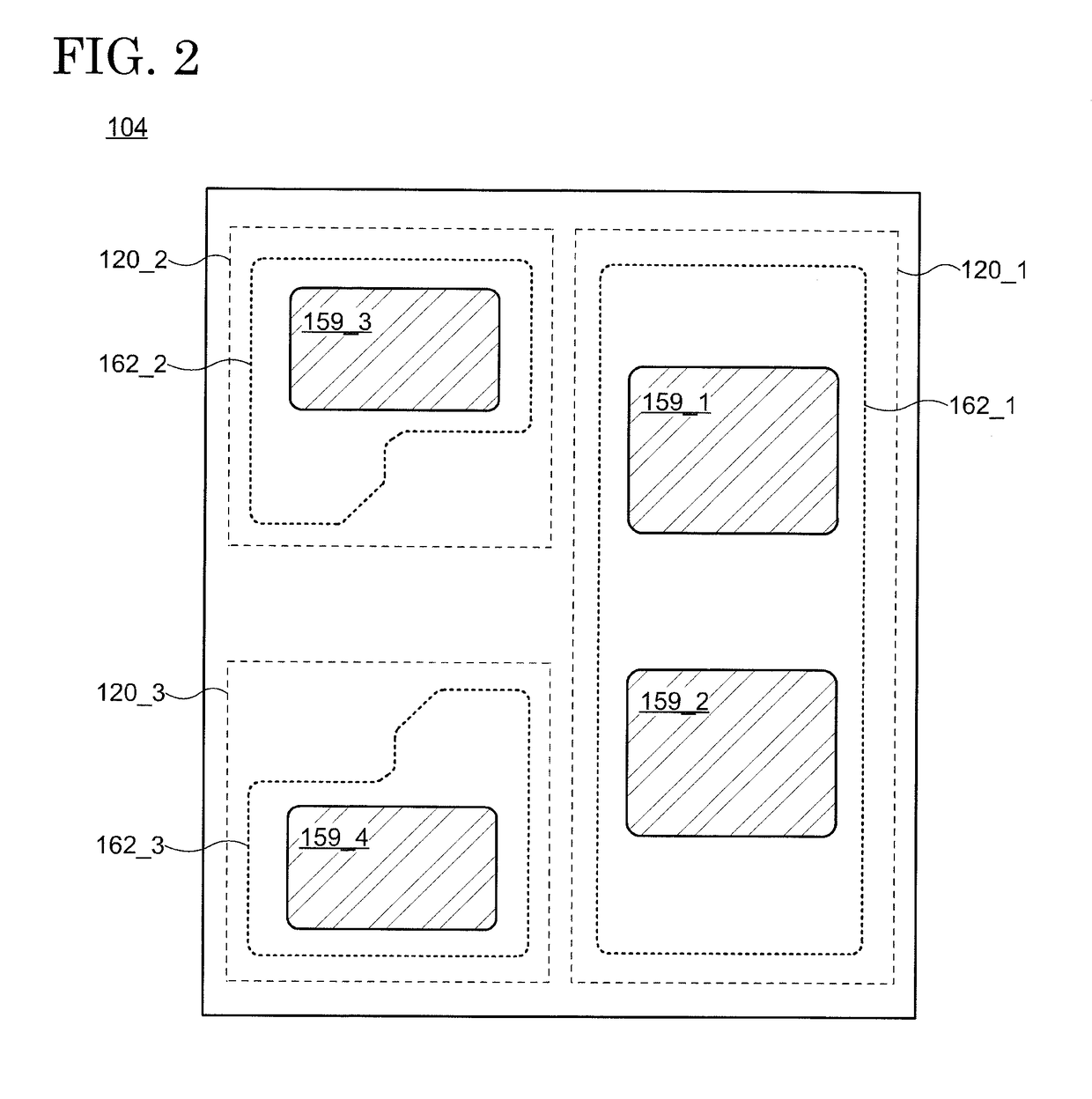
[0053]In the present embodiment, a pixel group 104a with a structure different from that of the pixel group 104 described in the First Embodiment is explained. An explanation regarding the structure the same as or similar to that of the pixel group 104 may be omitted.

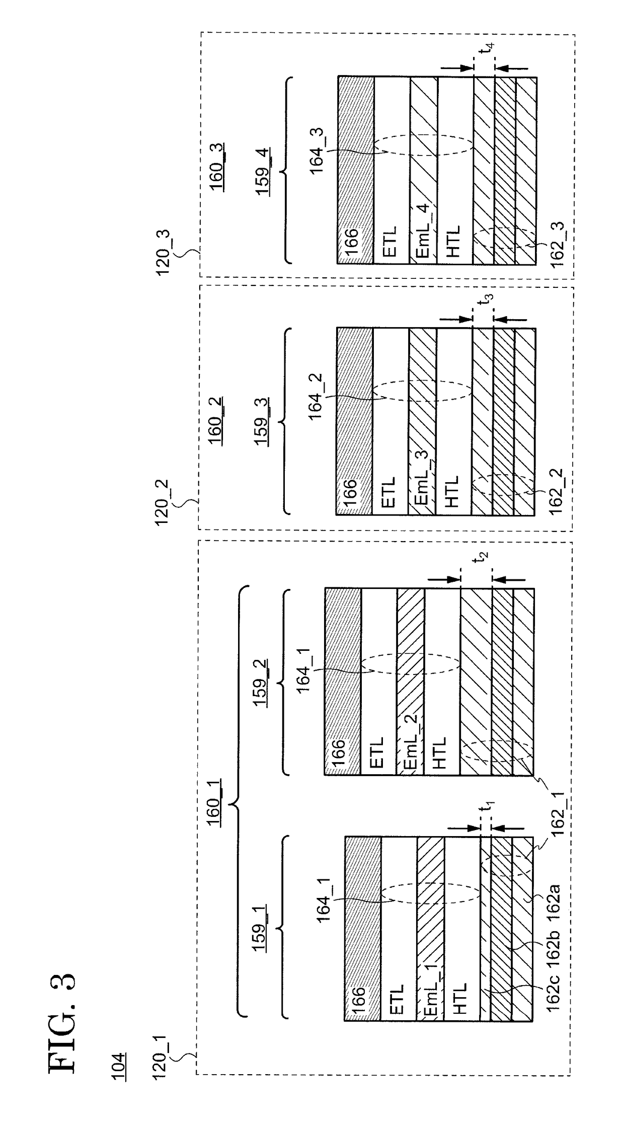
[0054]A schematic cross-sectional view of the pixel group 104a according to the present embodiment is shown in FIG. 6. The pixel group 104a is different from the pixel group 104 in that a thickness t4 of the third conductive layer 162c of the third light-emitting element 160_3 is larger than a thickness t3 of the third conductive layer 162c of the second light-emitting element 160_2. The thickness t3 is larger than the thickness t1 and smaller than the thickness t2. On the other hand, the thickness t4 may be the same as, larger than, or smaller than the thickness t2. Thus, one of the following relationships is satisfied.

t134≤t2

t1324

[0055]When the emission wavelength of the fourth electroluminescence layer 164_4 is lon...

third embodiment

[0056]In the present embodiment, a structure of the display device 100 and a manufacturing method thereof are explained. An explanation of the contents described in the First and Second Embodiments may be omitted.

1. Pixel Circuit

[0057]In each pixel 120, a variety of elements for driving the light-emitting element 160 is disposed in addition to the light-emitting element 160, by which a pixel circuit is fabricated. The structure of the pixel circuit may be arbitrarily selected, and an example is shown as an equivalent circuit in FIG. 7.

[0058]The pixel circuit shown in FIG. 7 includes a driving transistor 121, a first switching transistor 122, a second switching transistor 123, a storage capacitor 124, and a supplementary capacitor 125 in addition to the light-emitting element 160. The light-emitting element 160 is disposed between a high-potential power-source line 126 and a low-potential power-source line 127. The high-potential power-source line 126 is provided with a high potentia...


PUM


Abstract

Disclosed is a light-emitting element including a reflective electrode, a light-transmitting electrode over the reflective electrode, a partition wall over the light-transmitting electrode, the partition wall having a first opening and a second opening which overlap with the light-transmitting electrode, an electroluminescence layer over the first opening and the second opening, and an opposing electrode over the electroluminescence layer. A thickness of the light-transmitting electrode in a region overlapping with the first opening is smaller than a thickness of the light-transmitting electrode in a region overlapping with the second region.

Description

CROSS REFERENCE TO RELATED APPLICATIONS[0001]This application is based on and claims the benefit of priority from the prior Japanese Patent Application No. 2017-127204, filed on Jun. 29, 2017, the entire contents of which are incorporated herein by reference.FIELD[0002]The present invention relates to a display device and a manufacturing method of the display device. For example, the present invention relates to a display device having an organic light-emitting element in a pixel and a manufacturing method thereof.BACKGROUND[0003]An organic EL (Electroluminescence) display device is represented as an example of a display device. An organic EL display device has, as a display element, an organic light-emitting element (hereinafter, referred to as a light-emitting element) in each of a plurality of pixels formed over a substrate. A light-emitting element has a plurality of functional layers containing an organic compound (hereinafter, these functional layers are collectively referred ...

Claims


Application Information

Patent Timeline
IPC IPC(8): H01L51/52H01L27/32
CPCH01L51/5265H01L27/3246H01L51/5209H01L51/5215H01L2251/558H10K59/352H10K59/122H10K50/816H10K50/852H10K2102/351H10K50/813
Inventor TOYODA, HIRONORI
Owner JAPAN DISPLAY INC
Why Eureka
Try Eureka