
Semiconductor device and manufacturing method thereof

Active Publication Date: 2019-02-28
SK HYNIX INC
View PDF8 Cites 17 Cited by
  • Summary
  • Abstract
  • Description
  • Claims
  • Application Information

AI Technical Summary

Benefits of technology

This patent is about a semiconductor device that can be made with simple manufacturing processes, has a stable structure and improved performance. The patent also introduces a manufacturing method for this device.

Problems solved by technology

The increase in integration density of two-dimensional non-volatile memory devices in which memory cells are formed in a single layer over a substrate has recently been limited.

Method used


Image

  • Semiconductor device and manufacturing method thereof
  • Semiconductor device and manufacturing method thereof
  • Semiconductor device and manufacturing method thereof

Examples


Embodiment Construction

[0023]Hereinafter, various exemplary embodiments will be described in detail with reference to the accompanying drawings. In the drawings, thicknesses and lengths of components may be exaggerated for convenience of illustration. In the following description, a detailed description of related functions and constitutions may be omitted for simplicity and conciseness. Like reference numerals refer to like elements throughout the specification and drawings.

[0024]It is also noted that in this specification, “connected / coupled” refers to one component not only directly coupling another component but also indirectly coupling another component through an intermediate component. In addition, throughout the specification, when it is said that a certain part “includes” a certain element, this does not exclude other elements from being included but the certain part may further include another element unless particularly described otherwise.

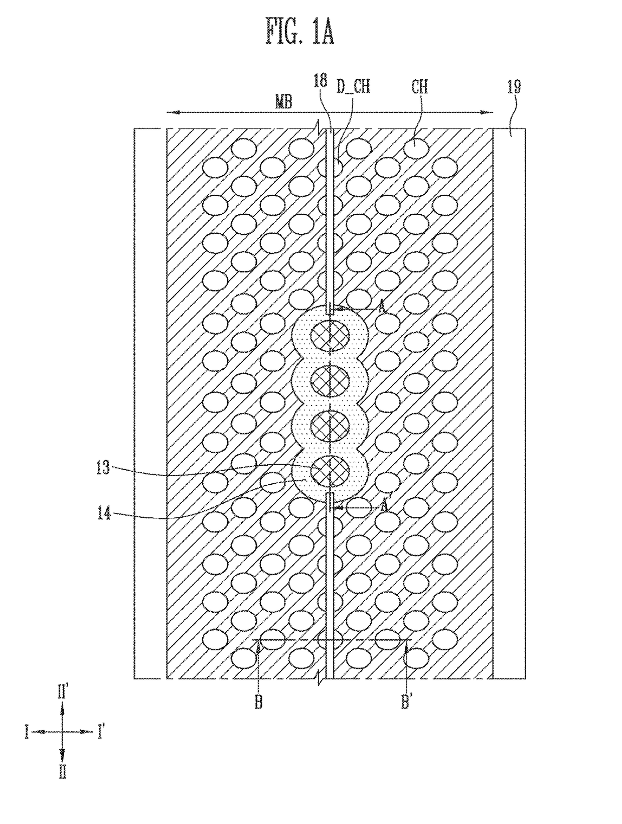
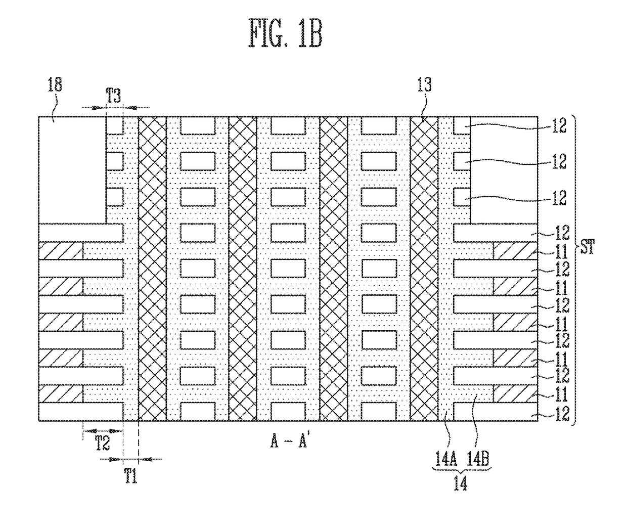
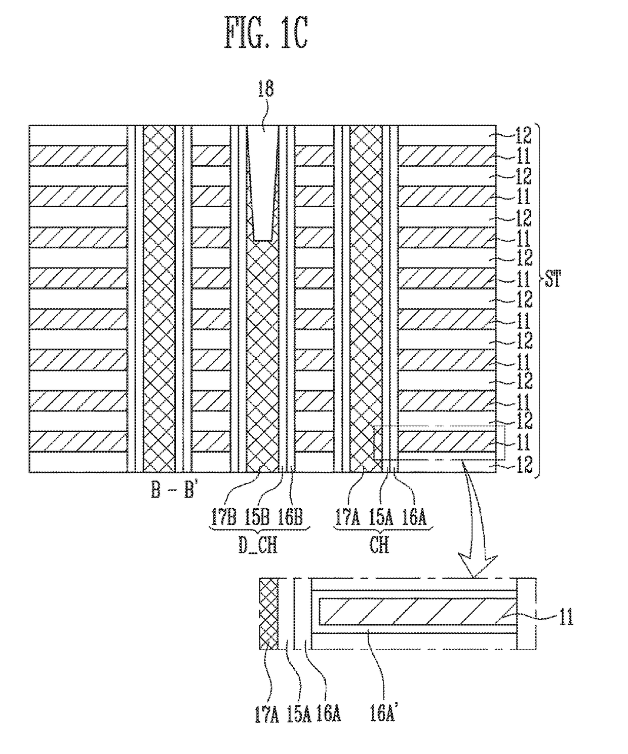
[0025]FIGS. 1A to 1C are diagram illustrating the struc...


PUM


Abstract

A semiconductor device includes a wiring structure, a stacked structure located over the wrong structure, channel structures passing through the stacked structure, contact plugs passing through the stacked structure and electrically connected to the wiring structure, and insulating spacers each including loop patterns surrounding a sidewall of each of the contact plugs and stacked along the side all of each of the contact plugs.

Description

CROSS-REFERENCE TO RELATED APPLICATION[0001]The present application claims priority under 35 U.S.C. § 119(a) to Korean patent application number 10-2017-0110971, filed on Aug. 31, 2017, and 10-2018-0023081, filed on Feb. 26, 2018, the entire disclosure of which is herein incorporated by reference in its entirety.BACKGROUNDField of Invention[0002]Various embodiments of the invention relate to an electronic device, and more particularly, to a semiconductor device and a manufacturing method thereof.Description of Related Art[0003]Non-volatile memory devices are used to store data which need to be maintained even in the absence of power supply. The increase in integration density of two-dimensional non-volatile memory devices in which memory cells are formed in a single layer over a substrate has recently been limited. Thus, three-dimensional non-volatile memory devices have been proposed in which memory cells are stacked in a vertical direction over a substrate.[0004]A three-dimensiona...

Claims


Application Information

Patent Timeline
IPC IPC(8): H01L23/528H01L23/532H01L23/535H01L29/06H01L21/768H01L21/311H01L21/762
CPCH01L23/528H01L23/53295H01L23/535H01L29/0649H01L21/76802H01L21/31116H01L21/76877H01L21/762H01L27/11556H01L27/11582H01L27/2454H10B41/20H10B63/30H10B63/845H10N70/25H10N70/823H10N70/231H10B41/10H10B41/40H10B41/35H10B43/10H10B43/40H10B41/27H10B43/35H10B43/27H10B63/34
Inventor LEE, KI HONG
Owner SK HYNIX INC
Learn More