Staggered Word Line Architecture for Reduced Disturb in 3-Dimensional NOR Memory Arrays

a technology of memory arrays and lines, applied in the direction of electrical equipment, semiconductor devices, instruments, etc., can solve the problems of sacrificing the density of memory arrays, and achieve the effect of avoiding the potential for disturbance, sacrificing memory cell density, and increasing the distance between such memory cells

Active Publication Date: 2019-02-28
SUNRISE MEMORY CORP
View PDF0 Cites 115 Cited by
  • Summary
  • Abstract
  • Description
  • Claims
  • Application Information

AI Technical Summary

Benefits of technology

[0005]The present invention avoids the potential for disturbs between memory cells in close proximity without sacrificing memory cell density. According to one embodiment of the present invention, a staggered memory cell architecture staggers memory cells on opposite sides of a shared bit line preserves memory cell density, while increasing the distance between such memory cell...

Problems solved by technology

However, with decreasing feature sizes, memory cells 1 and 2 are in close enough proximity that each memory cell may d...

Method used


Image

  • Staggered Word Line Architecture for Reduced Disturb in 3-Dimensional NOR Memory Arrays
  • Staggered Word Line Architecture for Reduced Disturb in 3-Dimensional NOR Memory Arrays
  • Staggered Word Line Architecture for Reduced Disturb in 3-Dimensional NOR Memory Arrays

Examples


Embodiment Construction

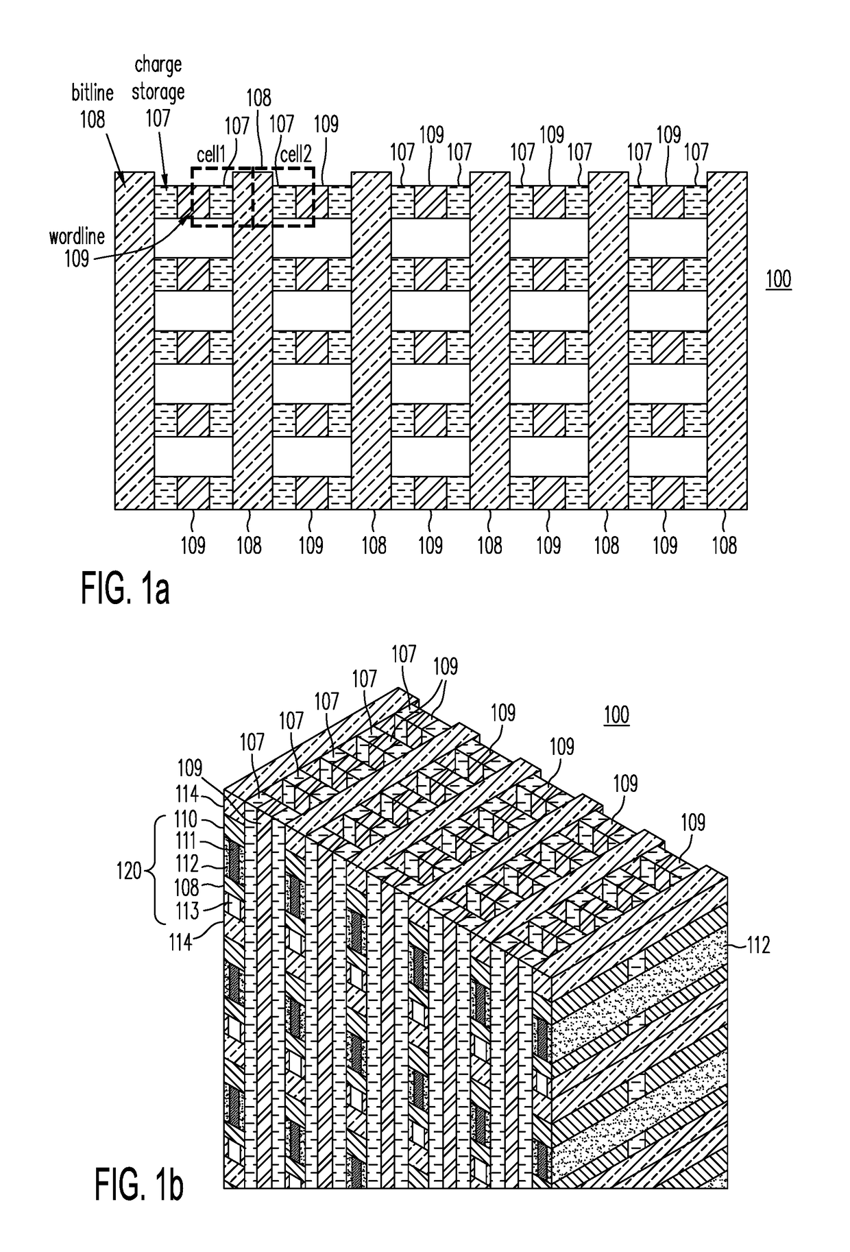
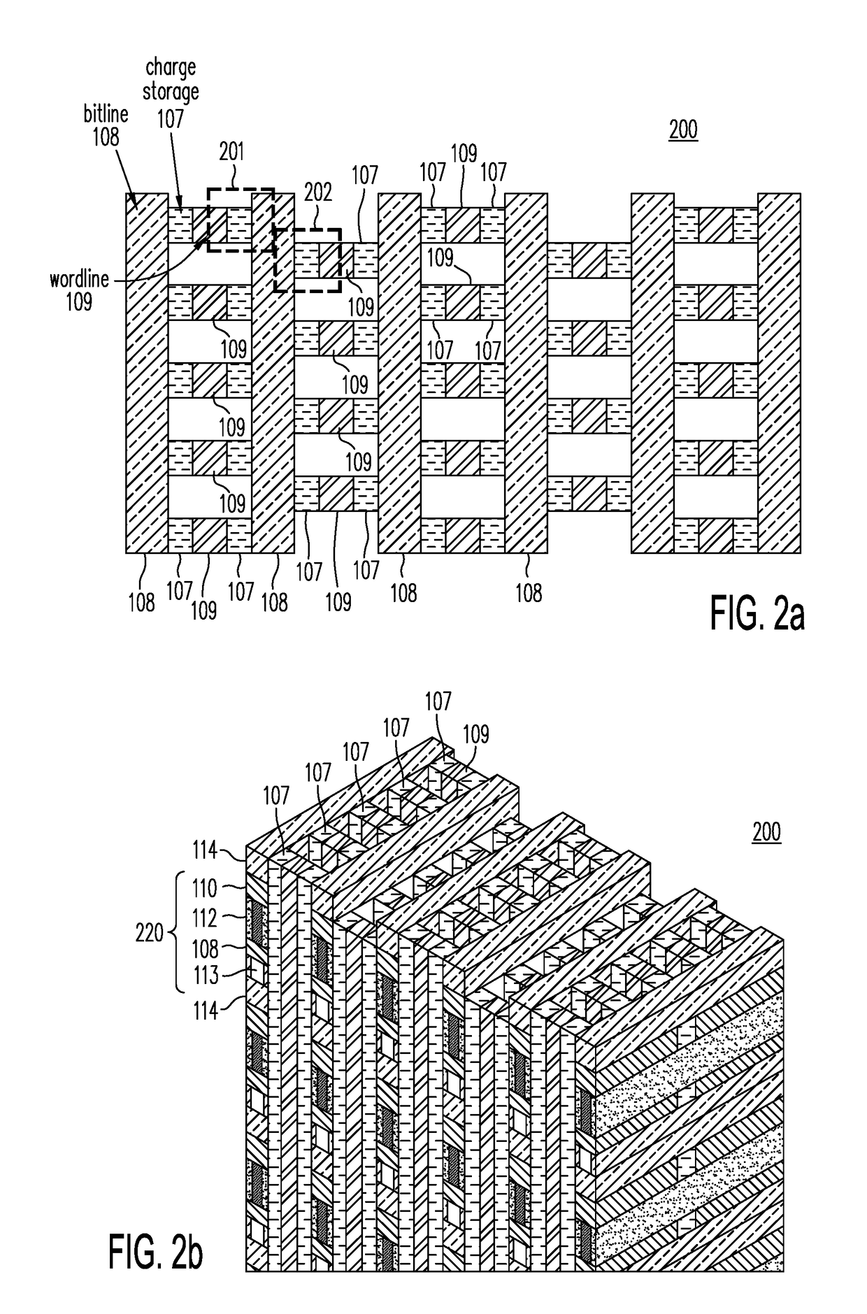
[0015]FIG. 2a show memory cells 201 and 202 of memory structure 200 on opposite side of shared bit line 108 being offset or “staggered” in position relative to each other, according to one embodiment of the present invention.

[0016]FIG. 2b shows completed memory structure 200 having staggered word lines in the manner illustrated in FIG. 2a. As in memory structure 100 of FIG. 1a, FIG. 1b shows completed memory structure 200 having word lines that are aligned in the manner illustrated in FIG. 2a. As shown in FIG. 2b, three-dimensional memory structure 200 includes a regular array of memory cells, each illustrated by memory cell 220. (Memory cell 220 shows in three dimensions each of memory cells 201 and 202.) In FIG. 2b, memory cell 220 includes channel region 112, which is provided between source region 110, drain region or bit line 108. In addition, memory cell 220 includes (i) charge-trapping material 107 provided between word line 109 and channel region 112, and (ii) conductor laye...


PUM


Abstract

A staggered memory cell architecture staggers memory cells on opposite sides of a shared bit line preserves memory cell density, while increasing the distance between such memory cells, thereby reducing the possibility of a disturb. In one implementation, the memory cells along a first side of a shared bit line are connected to a set of global word lines provided underneath the memory structure, while the memory cells on the other side of the shared bit line —which are staggered relative to the memory cells on the first side—are connected to global word lines above the memory structure.

Description

CROSS REFERENCES TO RELATED APPLICATIONS[0001]This application is related to and claims priority of U.S. provisional patent application (“Parent Application”), Ser. No. 62 / 551,110, entitled “Staggered Word Line Architecture for Reduced Disturb in 3-Dimensional NOR Memory Arrays,” filed on Aug. 28, 2017. This application is related to U.S. patent application (“Non-provisional Application”), Ser. No. 15 / 248,420, entitled “Capacitive-Coupled Non-Volatile Thin-film Transistor Strings in Three-Dimensional Arrays,” filed Aug. 26, 2016. The Non-provisional Application is hereby incorporated by reference in its entirety. The Non-provisional Application has been published as U.S. 2017 / 0092371. References to the Non-provisional Application herein are made by paragraph numbers of the publication. The present application is also related to (i) U.S. provisional application (“Provisional Application I”), Ser. No. 62 / 522,666, entitled “Replacement Metal and Strut for 3D memory Array,” filed on Jun...

Claims


Application Information

Patent Timeline
IPC IPC(8): H01L27/11582H01L27/11568H01L29/08
CPCH01L27/11582H01L27/11568H01L29/0847H01L29/7923G11C5/063G11C16/08H10B43/10H10B43/27H10B43/20H10B43/30
Inventor HERNER, SCOTT BRADHARARI, ELI
Owner SUNRISE MEMORY CORP
Why Eureka
Try Eureka