Display panel and method for manufacturing the same

a technology of display panel and display panel, which is applied in the direction of diodes, semiconductor devices, electrical devices, etc., can solve the problems of certain difficulties in the production of 300 ppi and more than 300 ppi products, self-luminous display panel, etc., to improve the light emission efficiency, reduce the color shifted phenomenon of self-luminous display panel, and optimize the process and yield of the panel

Inactive Publication Date: 2019-02-28
HKC CORP LTD +1
View PDF3 Cites 2 Cited by
  • Summary
  • Abstract
  • Description
  • Claims
  • Application Information

AI Technical Summary

Benefits of technology

[0008]In order to solve the above technical problems, it is an object of the present invention to provide a display panel and a method for manufacturing the same, by thinning the planarization layer corresponding to the light emitting region to raise the light emitting efficiency of the self-luminous display panel and to optimize the process and the yield of the panel, thereby the color shifted phenomenon of the self-luminous display panel is reduced.
[0029]The self-luminous display panel of the present invention employs the method of thinning the planarization layer corresponding to the light emitting region, it may raise the light emitting efficiency and optimize the process and the yield of the panel, and thereby the color shifted phenomenon of the self-luminous display panel is reduced.

Problems solved by technology

The existing technology used to define the resolution in the fabrication is mainly through the Side by Side technology, however, the technology has certain difficulty in the production of 300 ppi and more than 300 ppi products.
Such conventional method has a lot of the processes and the procedures are complex, in addition, since the one function of the planarization layer is used to support the pixel definition layer therefore once the relevant procedures for making the pixel definition layer are omitted, the displaying of the self-luminous display panel will be abnormal or color mixture and the illustrating performance is influenced.

Method used


Image

  • Display panel and method for manufacturing the same
  • Display panel and method for manufacturing the same
  • Display panel and method for manufacturing the same

Examples


Embodiment Construction

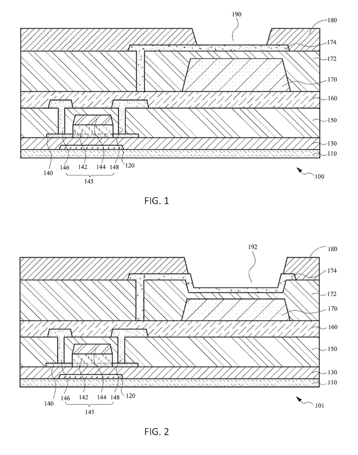
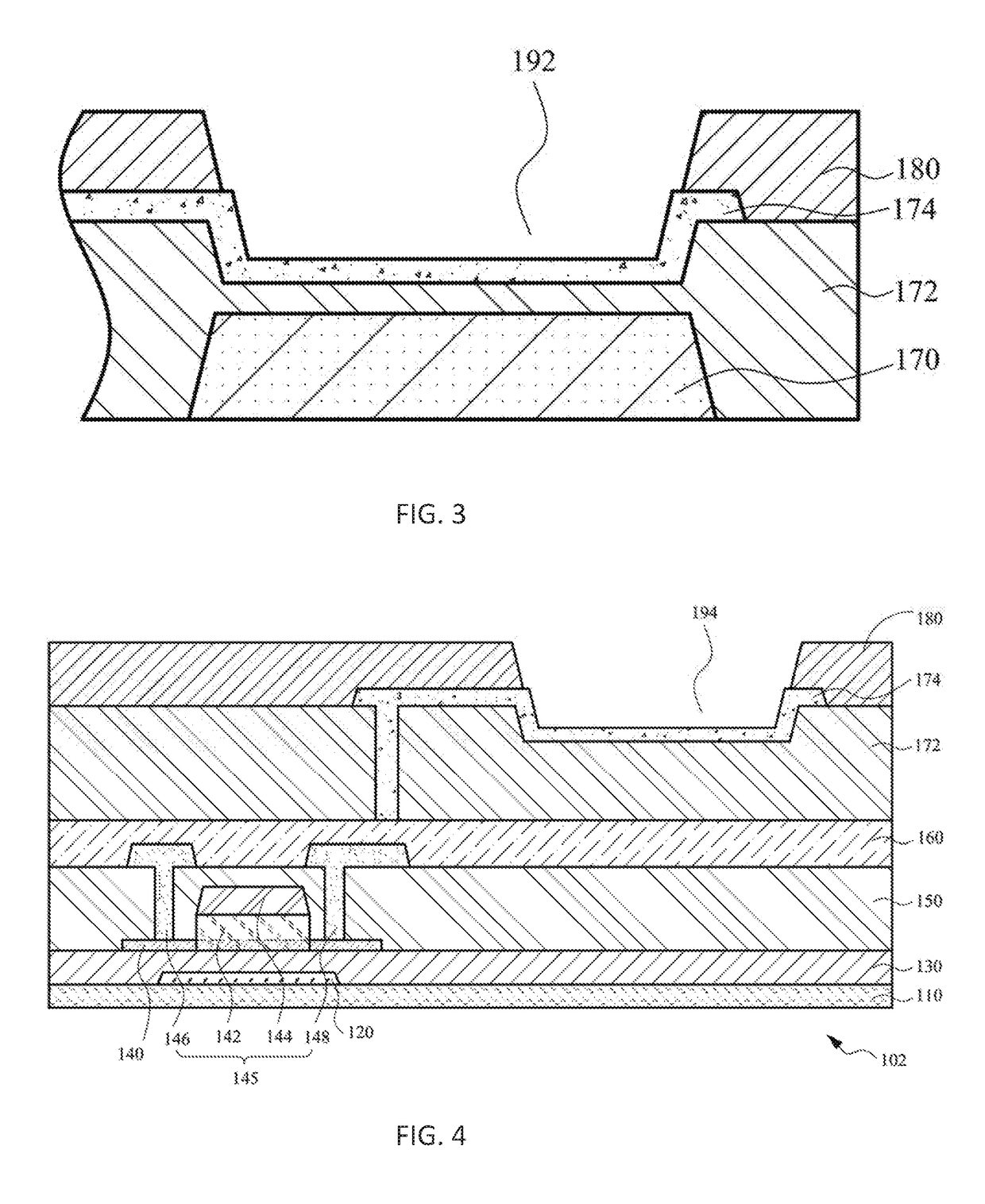
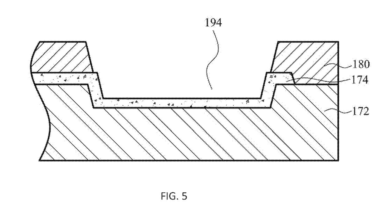
[0037]The following embodiments are referring to the accompanying drawings for exemplifying specific implementable embodiments of the present invention. Furthermore, directional terms described by the present invention, such as upper, lower, front, back, left, right, inner, outer, side and etc., are only directions by referring to the accompanying drawings, and thus the used directional terms are used to describe and understand the present invention, but the present invention is not limited thereto.

[0038]The drawings and description are to be regarded as illustrative in nature and not restrictive. Like reference numerals designate like elements throughout the specification. In addition, the size and thickness of each component shown in the drawings are arbitrarily shown for understanding and ease of description, but the present invention is not limited thereto.

[0039]In the drawings, the thickness of layers, films, panels, regions, etc., are exaggerated for clarity. In the drawings, ...


PUM


Abstract

A display panel comprises a substrate, a plurality of thin film transistors arranged on the substrate, a passivation layer disposed on the substrate and covering the plurality of thin film transistors, a pixel definition layer disposed on the passivation layer and configured to enable a plurality of light emitting elements to be disposed therein, a planarization layer disposed between the passivation layer and the pixel definition layer and having a groove structure, a color filter layer disposed between the passivation layer and the planarization layer and corresponding to the location of the groove structure, and a transparent electrode layer disposed on the planarization layer and covering the groove structure. Wherein the plurality of light emitting elements are disposed in the groove structure of the planarization layer and is aligned to the location of the color filter layer.

Description

FIELD OF THE INVENTION[0001]The present disclosure relates to a display panel and a method for manufacturing the same, and more particularly to an organic light-emitting diode display and a method for manufacturing the same.BACKGROUND OF THE INVENTION[0002]At present, the high resolution pixel flat display panel is a trend of the market, especially an active matrix organic light emitting diode (AMOLED) display panel is gaining interest and the AMOLED panel of a screen size of middle or small type with pixel density 200 ppi occupies a dominant position in the electronic display market. Also, an AMOLED with a wide video graphics array (WVGA) has gained popularity because of its resolution ratio higher than the VGA resolution ratio of 800*480 or about 200 ppi, and in the near future the developing trend of the display panel is toward to a higher resolution such as 250 ppi, 300 ppi and 350 ppi.[0003]The existing technology used to define the resolution in the fabrication is mainly throu...

Claims


Application Information

Patent Timeline
Patent Type & Authority Applications(United States)
IPC IPC(8): H01L27/32H01L51/56
CPCH01L27/3258H01L27/322H01L27/3246H01L27/3262H01L51/56H01L27/1248H01L27/1225H01L29/24H01L29/45H01L29/7869H01L27/1288H01L2227/323H10K59/38H10K59/124H10K59/126H10K59/122H10K59/1213H10K71/00H10K59/1201
Inventor CHO, EN-TSUNGTIAN, YIQUNYANG, FENGYUNFAN, KUN
Owner HKC CORP LTD
Why Eureka
Try Eureka