Array substrate and display panel

Active Publication Date: 2019-03-28
WUHAN CHINA STAR OPTOELECTRONICS TECH CO LTD
View PDF4 Cites 1 Cited by
  • Summary
  • Abstract
  • Description
  • Claims
  • Application Information

AI Technical Summary

Benefits of technology

The patent text describes a display panel that has uneven pixel voltage, which causes whitening issues at the edges of the panel. The technical effect of the patent is to reduce the pixel voltage of the pixels in the second area, which is farther from the input end of scanning signals, to equalize the pixel voltage across the entire panel and improve display performance. This results in a more uniform display and better overall performance of the display panel.

Problems solved by technology

However, the signals may have time difference between the starting end and the terminal end of the scanning line due to the time-delay of the resistor and the capacitor, resulting in an impact on the pixel voltages of the pixel cells on the starting end and the terminal end.
When the size of the panel becomes larger and the scanning line becomes longer, the time-delay of the resistor and the capacitor may become greater.
As such, the brightness of the both sides of the display panel may be greater than that of the center of the panel, resulting in a non-uniform display.

Method used


Image

  • Array substrate and display panel
  • Array substrate and display panel
  • Array substrate and display panel

Examples


Embodiment Construction

[0014]To clarify the purpose, technical solutions, and the advantages of the disclosure, embodiments of the invention will now be described more fully hereinafter with reference to the accompanying drawings.

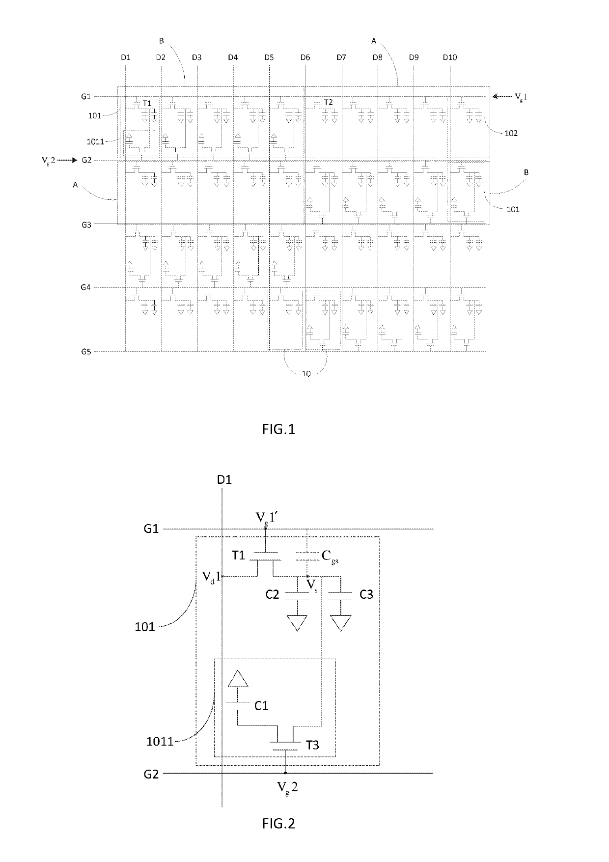
[0015]Referring to FIG. 1, the present disclosure relates to an array substrate, including: a plurality of scanning lines Gn (for example G1, G2, G3, G4 and G5 in the present embodiment), a plurality of data lines Dn (for example D1, D2, D3, D4, D5, D6, D7, D8, D9 and D10 in the present embodiment). The data lines Dn and the scanning lines Gn respectively intersect with each other to form a plurality of pixel cells 10.

[0016]The pixel cells 10 may be divided into the pixel cells within a first area (A) and the pixel cells within a second area (B) along a direction of the scanning lines Gn. A distance between the first area (A) and an input end of scanning signals is less than a distance between the second area (B) and the input end of the scanning signals. Each of the pixel cells ...


PUM


Abstract

The present disclosure relates to an array substrate and a display panel. The array substrate includes a plurality of scanning lines and a plurality of data lines intersecting with each other to form a plurality of pixel cells. The pixel cells are divided into the pixel cells within a first area and the pixel cells within a second area along the scanning lines. Each of the pixel cells within the second area includes a first thin film transistor (TFT) and a control unit connected to the first TFT. The control unit is configured to reduce a pixel voltage of the pixel cell where the first TFT is configured. As such, the display panel may display images uniformly, and display performance of the display panel may be improved.

Description

BACKGROUND1. Technical Field[0001]The present disclosure relates to a display field, and more particularly to an array substrate and a display panel.2. Description of Related Art[0002]The thin film transistor (TFT) adopted in display devices mainly includes amorphous silicon TFTs and poly-silicon TFTs. With the increasing of the using time, mobility and photosensitivity of the amorphous silicon TFTs may be largely reduced. However, the low temperature poly-silicon (LTPS) may have better mobility and stability when comparing with the amorphous silicon.[0003]The gate driver on array (GOA) of the LTPS panels usually adopts the one-way driving interlaced scanning mode. That is, the gate drivers are configured on both sides of the LTPS panel, and the gate drivers may be turned on according to the scanning timings of the scanning lines. However, the signals may have time difference between the starting end and the terminal end of the scanning line due to the time-delay of the resistor and...

Claims


Application Information

Patent Timeline
IPC IPC(8): G09G3/36H01L27/12G02F1/1368G02F1/1362
CPCG09G3/3648G09G3/3677H01L27/124G02F1/1368H01L27/1255G02F1/136286G09G2320/0233G09G2300/0819G02F1/1362G09G2300/0852G09G2300/0426G02F1/13624G09G3/3659
Inventor ZHANG, TINGTINGWANG, CONG
Owner WUHAN CHINA STAR OPTOELECTRONICS TECH CO LTD
Why Eureka
Try Eureka