
Solid state image sensor with on-chip filter and extended spectral response

Active Publication Date: 2019-03-28
QUALCOMM INC
View PDF6 Cites 6 Cited by
  • Summary
  • Abstract
  • Description
  • Claims
  • Application Information

AI Technical Summary

Benefits of technology

The patent describes an image sensor with an extended spectral response that includes a first sensor portion and a second sensor portion positioned on top of each other. The first sensor portion includes a first photodetector and a first metal-interconnect layer, while the second sensor portion includes a second photodetector and a second metal-interconnect layer. The image sensor may also include a dual bandpass filter or a narrow bandpass filter. The image sensor can capture images with light within different wavelength ranges. The technical effect of this invention is to provide an image sensor with improved sensitivity and accuracy in capturing images.

Problems solved by technology

While each of the FSI and BSI image sensors have favorable imaging characteristics, they both have limited spectral responses.

Method used


Image

  • Solid state image sensor with on-chip filter and extended spectral response
  • Solid state image sensor with on-chip filter and extended spectral response
  • Solid state image sensor with on-chip filter and extended spectral response

Examples


Embodiment Construction

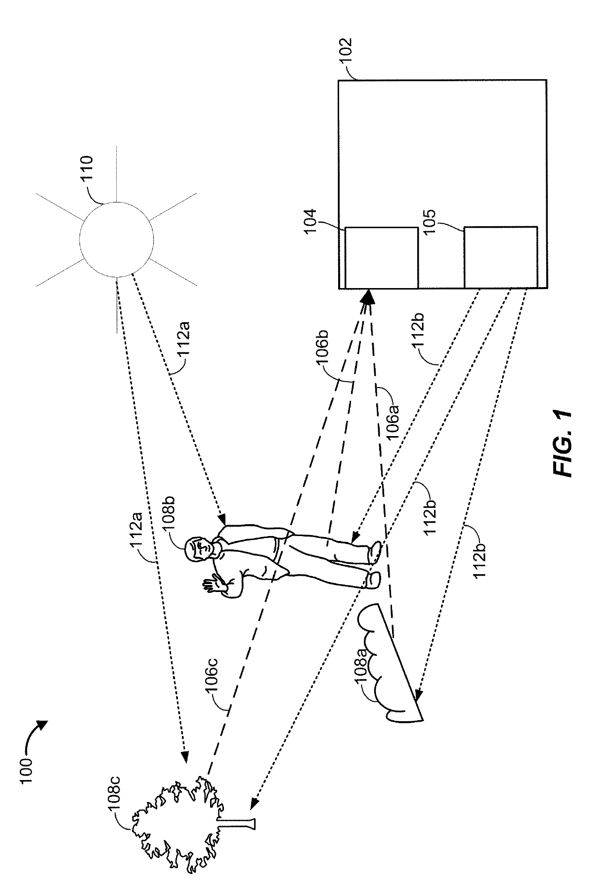
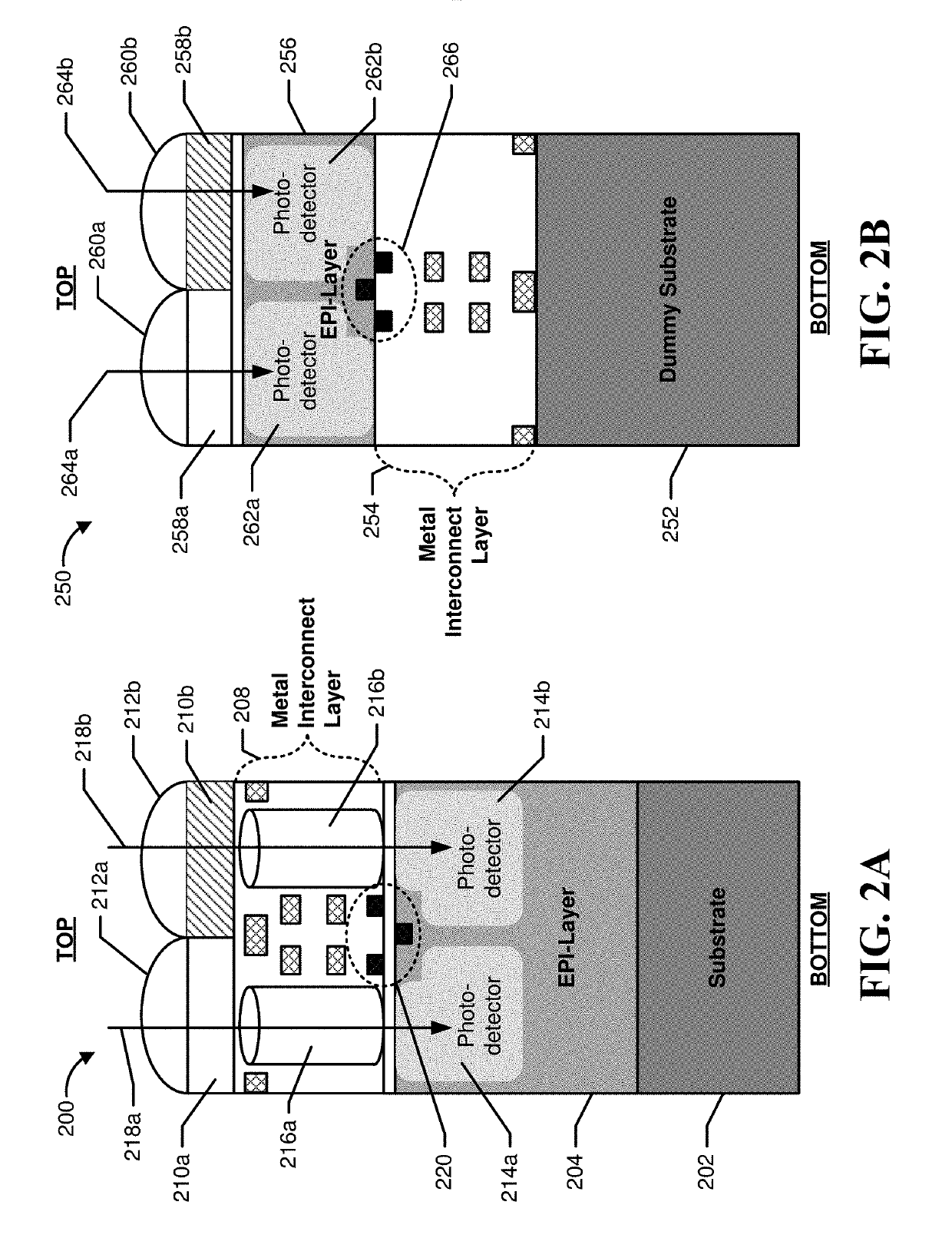
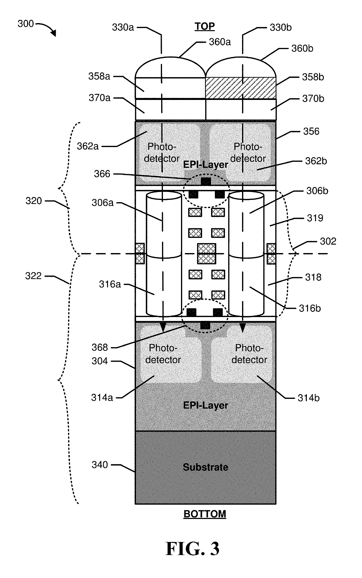
[0037]As described herein, some components of an image sensor (e.g., an FSI or BSI image sensor) may sometimes be referred to as positioned “above,”“on top of,”“underneath”, “below,” or similar terminology in relation to some other components. For ease of description, spatial relations between components in an image sensor may be described in relation to the “top” and “bottom” of the image sensor. In some embodiments, the “top” of an image sensor may correspond with the point at which light initially strikes and / or enters the image sensor. Accordingly, the “bottom” of the image sensor may be on the opposite side of the image sensor than the top of the image sensor. Thus, a second component or element of an image sensor that is closer to the top of the image sensor than a first component may be described as being “on top of” or “above” the first component.

[0038]In embodiments described herein, certain references to an image sensor as having a “first sensor portion” (or a “first image...


PUM


Abstract

Various embodiments are directed to an image sensor that includes a first sensor portion and a second sensor portion. The second sensor portion may be positioned relative to the first sensor portion such that the second sensor portion may initially detect light entering the image sensor, and some of that light passes through the second sensor portion and may be detected by the first sensor portion. In some embodiments, one more optical filters may be disposed within the image sensor. The one or more optical filters may include at least one of a dual bandpass filter disposed above the second photodetector or a narrow bandpass filter disposed between the first photodetector and the second photodetector.

Description

TECHNICAL FIELD[0001]This disclosure relates to an image sensor, and specifically to an image sensor with an on-chip filter having an extended spectral range.BACKGROUND[0002]Image processing devices, such as digital cameras, smartphones or tablet computers, rely on image sensors to capture images. Image sensors receive light and convert that light into electrical signals. The image processing devices then transform these electrical signals into digital images.[0003]Different types of image sensors are currently available. For example, image processing devices typically utilize either a frontside-illumination (FSI) image sensor or a backside-illumination (BSI) image sensor. An FSI image sensor is typically oriented such that light enters the top of the FSI image sensor and passes through a metal-interconnect layer before striking a light-sensing surface. In contrast, BSI image sensors are oriented to allow light to enter from the top of the BSI image sensor and to strike a light-sens...

Claims


Application Information

Patent Timeline
IPC IPC(8): H01L27/146H01L31/0216H04N5/374
CPCH01L27/14605H01L27/1464H01L27/14636H01L27/14625H01L27/14645H01L27/14649H01L31/02165H04N5/374H01L27/14627H01L27/14621G01J1/16G01J3/0205G01J3/36G01J2001/1652G01J3/0208G01J1/0488H01L27/14612H01L27/14629H01L27/14634H04N25/76
Inventor HSEIH, BIAY-CHENGGEORGIEV, TODOR GEORGIEVMAGOMA, SERGIU
Owner QUALCOMM INC
Features
  • Generate Ideas
  • Intellectual Property
  • Life Sciences
  • Materials
  • Tech Scout
  • Unparalleled Data Quality
  • Higher Quality Content
  • 60% Fewer Hallucinations
Learn More