
Capacitive touch sensing circuit and charge compensation method thereof

a capacitive touch and circuit technology, applied in the field of touch panels, can solve the problems of large increase in the area of compensation capacitors, and achieve the effects of reducing compensation capacitance area, small capacitance, and effective offset of relatively large external capacitan

Active Publication Date: 2019-04-11
RAYDIUM SEMICON
View PDF34 Cites 1 Cited by
  • Summary
  • Abstract
  • Description
  • Claims
  • Application Information

AI Technical Summary

Benefits of technology

The present invention is about a new method for compensating for electrodes in a capacitive touch panel. This method uses a charge compensation mechanism to effectively offset the large external capacitance by the small capacitance inside the circuit. This allows for better sensing of touch even in heavy load environments. Additionally, this method reduces the compensation capacitance area required in the circuit and improves the internal capacitance sensing range.

Problems solved by technology

However, as the external capacitance increases, the internal pre-filled capacitor must also increase with the same amount, resulting in a large increase in the area of the compensation capacitor required in the capacitive touch sensing circuit, which needs to be overcome.

Method used

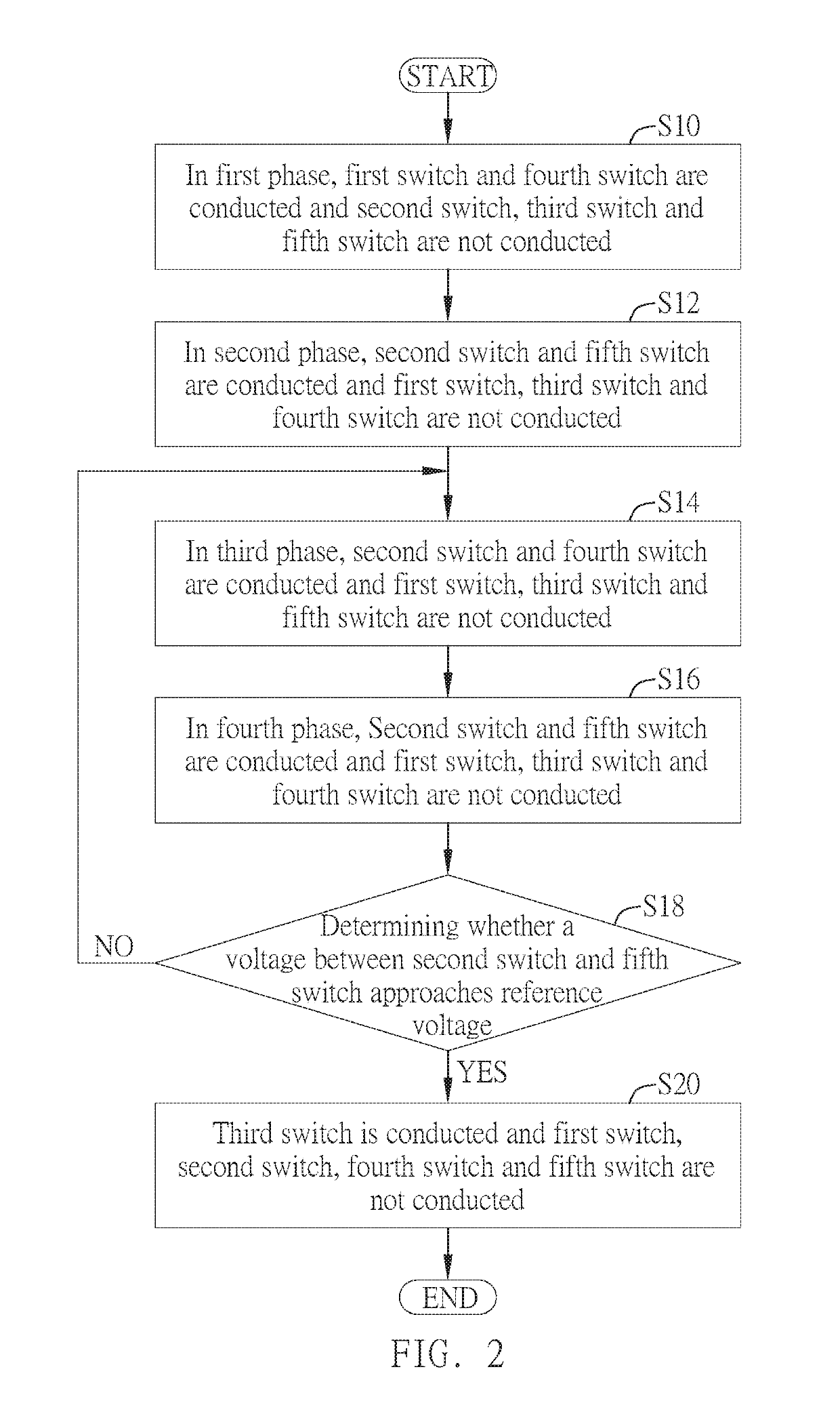
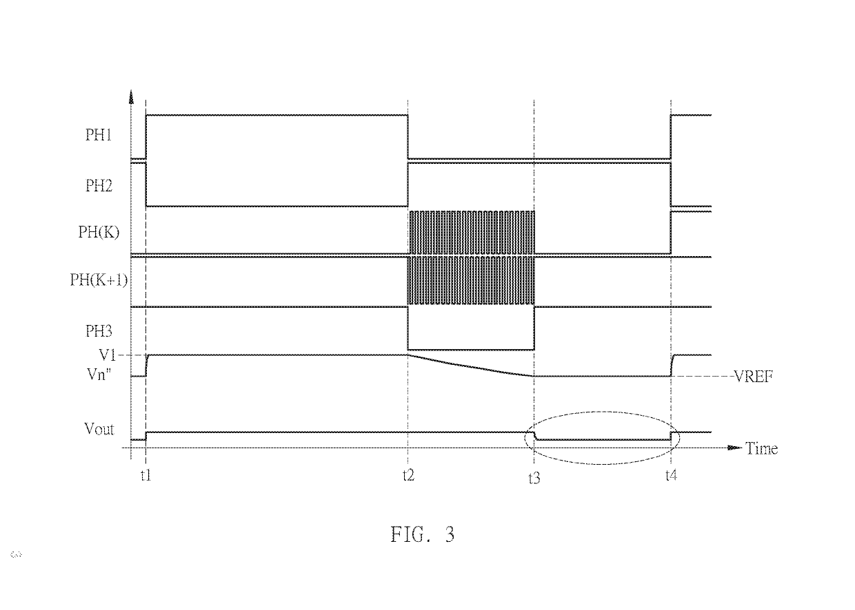

Image

  • Capacitive touch sensing circuit and charge compensation method thereof
  • Capacitive touch sensing circuit and charge compensation method thereof
  • Capacitive touch sensing circuit and charge compensation method thereof

Examples


Embodiment Construction

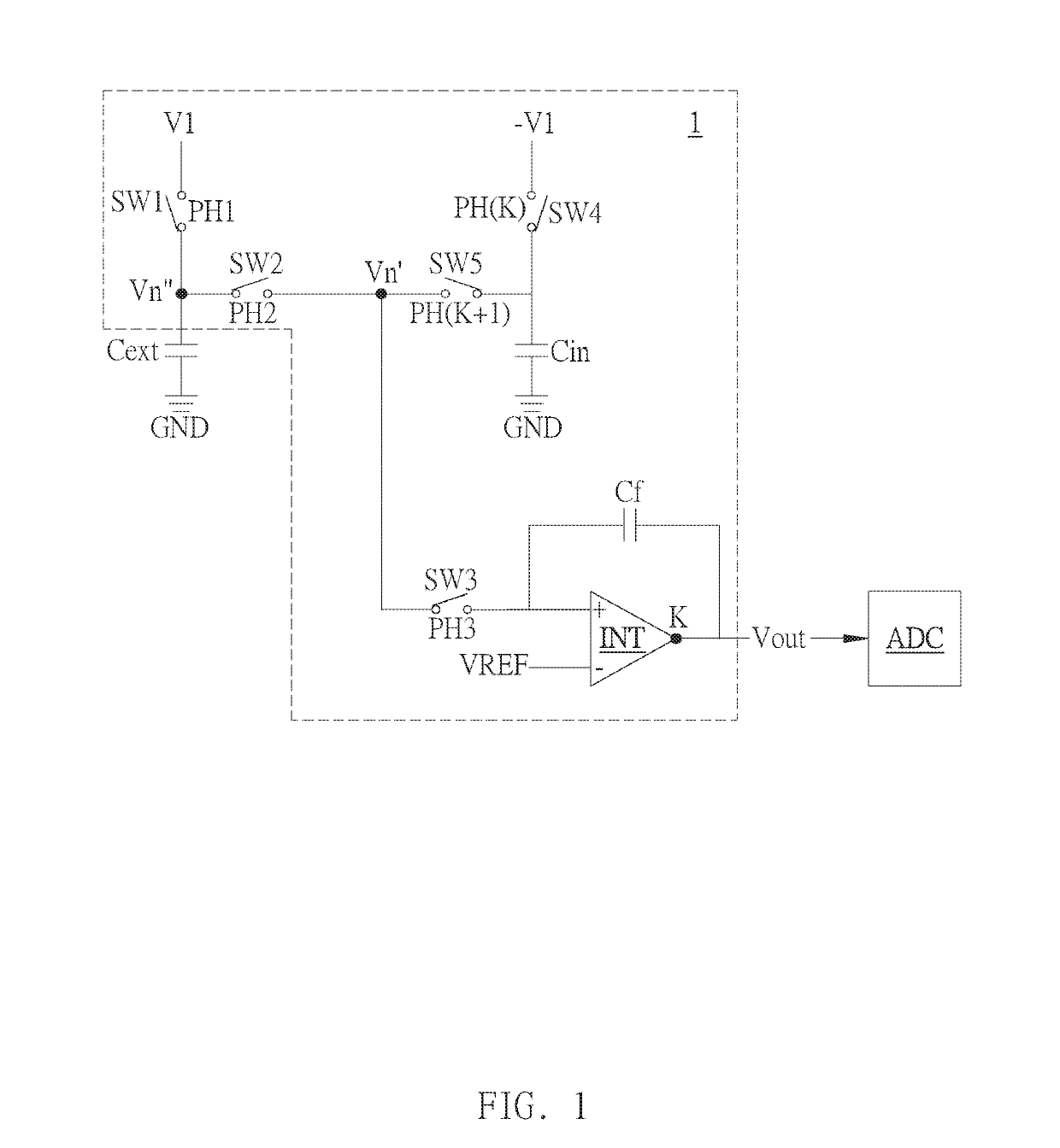
[0020]A preferred embodiment of the invention is a capacitive touch sensing circuit applied to a capacitive touch panel. In this embodiment, the capacitive touch sensing circuit is configured to sense a capacitance change of an external capacitance to be detected when the capacitive touch panel is touched and to suppress external environmental noise. The structure of the capacitive touch panel can be designed in different types such as in-cell, on-cell or out-cell.

[0021]Please refer to FIG. 1. FIG. 1 illustrates a schematic diagram of the capacitive touch sensing circuit in this embodiment.

[0022]As shown in FIG. 1, the capacitive touch sensing circuit 1 is coupled to an external capacitor Cext to be detected and an analog-to-digital converter ADC. The capacitive touch sensing circuit 1 includes a first switch SW1, a second switch SW2, a third switch SW3, a fourth switch SW4, a fifth switch SW5, an internal capacitor Cin, an integrator INT and a capacitor Cf. The first switch SW1, th...


PUM


Abstract

A capacitive touch sensing circuit includes a first switch˜a fifth switch, an internal capacitor, an integrator and a capacitor. The first switch and an external capacitor are coupled in series between a first voltage and a ground voltage, one terminal of the second switch is coupled between the first switch and the external capacitor, and one terminal of the third switch is coupled to the other terminal of the second switch. The fourth switch and the internal capacitor are coupled in series between a second voltage and the ground voltage, wherein the second voltage is a negative value of the first voltage, and one terminal of the fifth switch is coupled to the other terminal of the second switch and the other terminal of the fifth switch is coupled between the fourth switch and the internal capacitor. One input terminal of the integrator is coupled to the other terminal of the third switch, the other input terminal of the integrator is coupled to a reference voltage, and the output terminal of the integrator outputs an output voltage. The capacitor is coupled between the input terminal and the output terminal of the integrator.

Description

BACKGROUND OF THE INVENTION1. Field of the Invention[0001]The invention relates to a touch panel; in particular, to a capacitive touch sensing circuit and a charge compensation method thereof applied to a capacitive touch panel.2. Description of the Prior Art[0002]In general, the capacitive touch panel can be designed in different types such as in-cell, on-cell or out-cell. In the process of using a capacitive touch panel, it is generally necessary to offset the external capacitor to improve the internal charge detection range.[0003]However, as the external capacitance increases, the internal pre-filled capacitor must also increase with the same amount, resulting in a large increase in the area of the compensation capacitor required in the capacitive touch sensing circuit, which needs to be overcome.SUMMARY OF THE INVENTION[0004]Therefore, the invention provides a capacitive touch sensing circuit and a charge compensation method thereof applied to a capacitive touch panel to solve t...

Claims


Application Information

Patent Timeline
Patent Type & Authority Applications(United States)
IPC IPC(8): G06F3/041G06F3/044H03K17/96
CPCG06F3/0418G06F3/044H03K17/962H03K2217/960725
Inventor CHEN, CHIH-HSIUNGHSU, YU-CHINYUAN, CHIH
Owner RAYDIUM SEMICON
Learn More