
Electro-optic displays, and methods for driving same

a technology of electrophoretic displays and optical displays, applied in the direction of non-linear optics, static indicating devices, instruments, etc., can solve the problems of display presenting a kickback/self-erasing or self-improving phenomenon, impulse switching models can lose accuracy at low voltage, and display may present a long-term lifetime degradation. , to achieve the effect of shortening the display pixel

Inactive Publication Date: 2019-04-11
E INK CORPORATION
View PDF8 Cites 4 Cited by
  • Summary
  • Abstract
  • Description
  • Claims
  • Application Information

AI Technical Summary

Benefits of technology

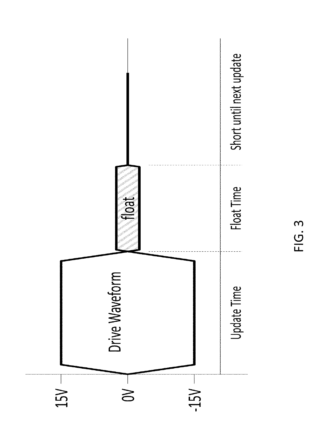
The patent describes a way to drive a display pixel by applying a waveform, keeping it in a floating state, and then briefly shorting it. The technical effect of this method is to improve the display's image quality and resolution.

Problems solved by technology

It has also been found that DC imbalances may cause long-term lifetime degradation of some electrophoretic displays.
In practice, however, the impulse switching model can lose accuracy at low voltages.
If the threshold is inadequate or if the remnant voltage is too high, the display may present a kickback / self-erasing or self-improving phenomenon.
Even when remnant voltages are below a small threshold, they may have a serious effect on image switching if they still persist when the next image update occurs.
Furthermore, this effect varies with elapsed time due to the decay rate of the remnant voltage.
In practical terms then, the most noticeable effect of remnant voltage on display performance may be ghosting.
This problem is in addition to the problem previously noted, namely that DC imbalance (e.g. 16 V / 14 V instead of 15 V / 15 V) may be a cause of slow lifetime degradation of the electro-optic medium.
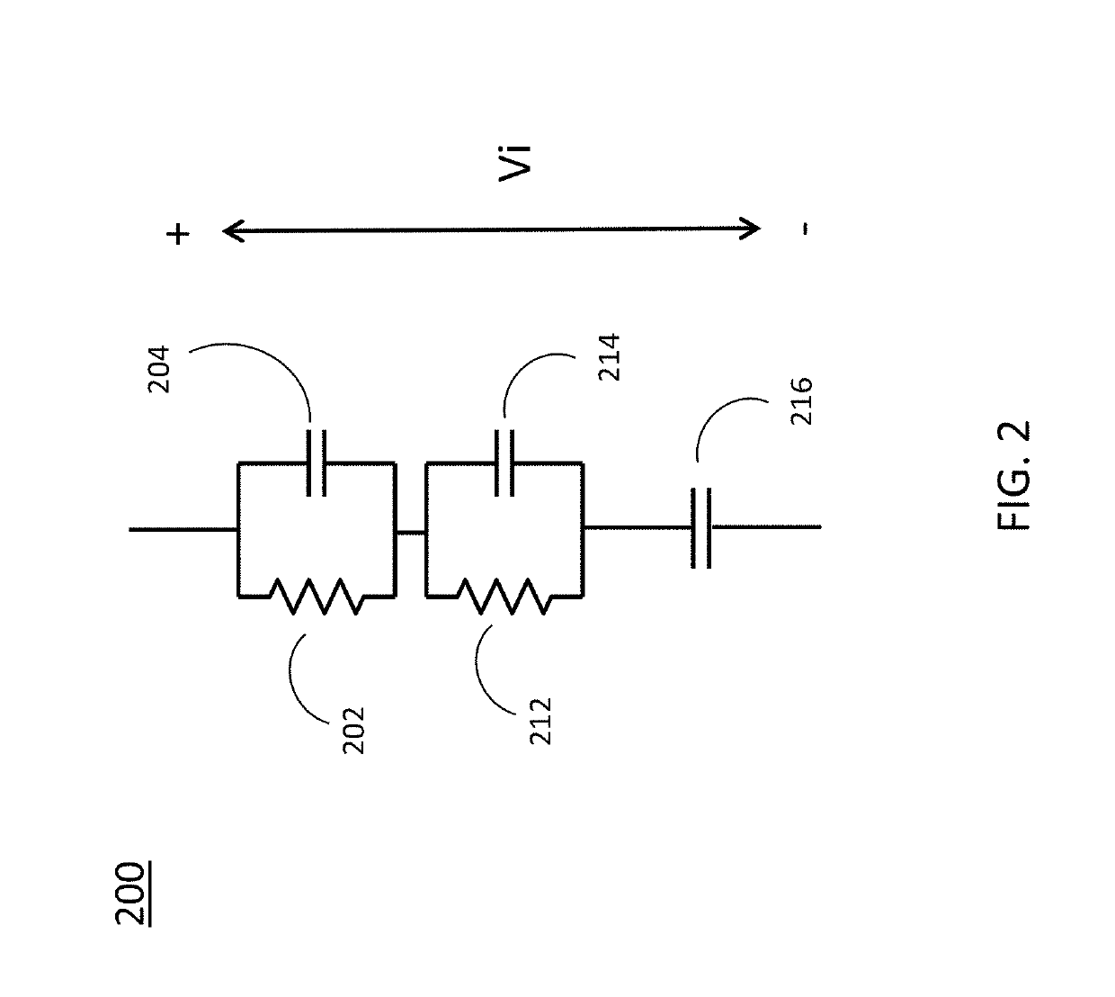
It is believed (although some embodiments are in no way limited by this belief), that one large cause of remnant voltage is ionic polarization within the materials of the various layers forming the display.
Remnant voltage can also create a DC imbalance and reduce ultimate display lifetime.
The effects of remnant voltage therefore may be deleterious to the quality of the electrophoretic or other electro-optic device and it is desirable to minimize both the remnant voltage itself, and the sensitivity of the optical states of the device to the influence of the remnant voltage.
That is, conventional techniques of discharging the remnant voltage may result in the electro-optic display retaining at least a low remnant voltage.

Method used


Image

  • Electro-optic displays, and methods for driving same
  • Electro-optic displays, and methods for driving same
  • Electro-optic displays, and methods for driving same

Examples


Embodiment Construction

[0020]The term “electro-optic”, as applied to a material or a display, is used herein in its conventional meaning in the imaging art to refer to a material having first and second display states differing in at least one optical property, the material being changed from its first to its second display state by application of an electric field to the material. Although the optical property is typically color perceptible to the human eye, it may be another optical property, such as optical transmission, reflectance, luminescence or, in the case of displays intended for machine reading, pseudo-color in the sense of a change in reflectance of electromagnetic wavelengths outside the visible range.

[0021]The term “gray state” is used herein in its conventional meaning in the imaging art to refer to a state intermediate two extreme optical states of a pixel, and does not necessarily imply a black-white transition between these two extreme states. For example, several of the E Ink patents an...


PUM


Abstract

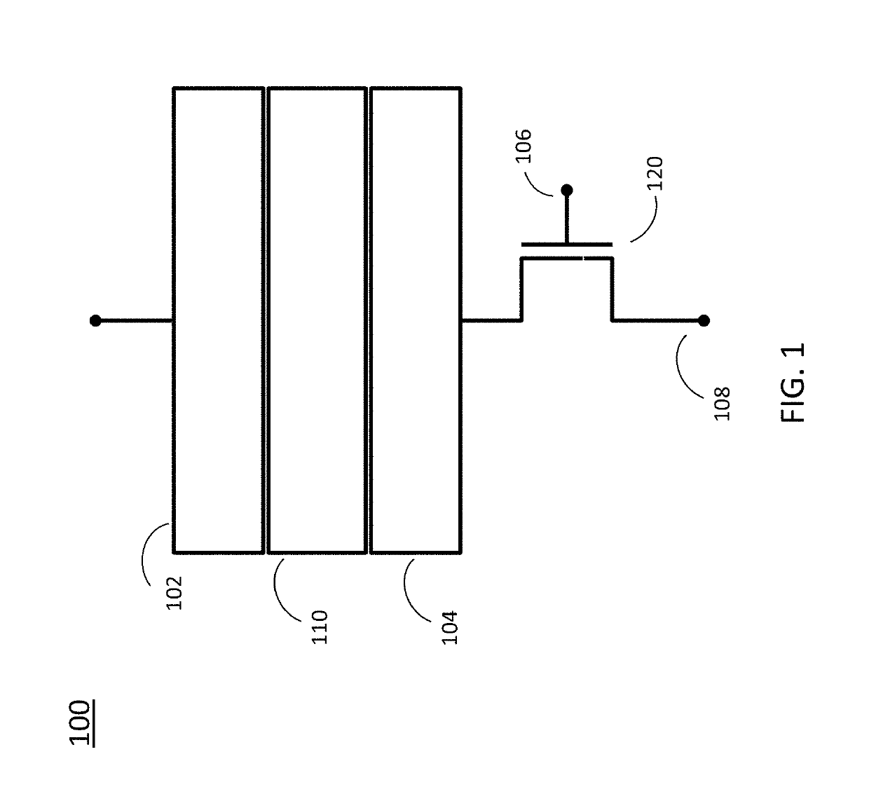
A method for driving a display having at least one display pixel is provided, the method may include applying a waveform to the at least one display pixel, maintaining a floating state on the display pixel, and shorting the display pixel.

Description

REFERENCE TO RELATED APPLICATIONS[0001]This application is related to and claims priority of U.S. Provisional Application 62 / 536,301 filed on Jul. 24, 2017. The entire disclosure of the aforementioned application is herein incorporated by reference.SUBJECT OF THE INVENTION[0002]This invention relates to reflective electro-optic displays and materials for use in such displays. More specifically, this invention relates to displays with reduced remnant voltage and driving methods for reducing remnant voltage in electro-optic displays.BACKGROUND[0003]Electro-optics displays driven by direct current (DC) imbalanced waveforms may produce a remnant voltage, this remnant voltage being ascertainable by measuring the open-circuit electrochemical potential of a display pixel. It has been found that remnant voltage is a more general phenomenon in electrophoretic and other impulse-driven electro-optic displays, both in cause(s) and effect(s). It has also been found that DC imbalances may cause l...

Claims


Application Information

Patent Timeline
Patent Type & Authority Applications(United States)
IPC IPC(8): G09G3/34
CPCG09G3/344G09G2320/043G09G2320/0204G09G2310/06G09G2310/065G02F1/1685G02F1/167G09G2230/00G09G2310/0264G09G3/34
Inventor LAUBER, DAN JOHNMILLER, DAVID DARRELLLAN, WENJIELU, YI
Owner E INK CORPORATION
Learn More