Display apparatus

a display apparatus and display technology, applied in the field of display apparatuses, can solve problems such as loss of normal transistor characteristics, and achieve the effects of reducing the desorption of oxygen from the channel material of the transistor, prolonging the service life of the display apparatus, and increasing the regular operation period of the transistor

Inactive Publication Date: 2010-11-18
SONY CORP
View PDF10 Cites 16 Cited by
  • Summary
  • Abstract
  • Description
  • Claims
  • Application Information

AI Technical Summary

Benefits of technology

[0052]Further, inappropriate operation upon threshold value correction and mobility correction which may possibly occur in the signal gate structure of an oxide semiconductor transistor can be eliminated.
[0053]With the display apparatus, since each pixel circuit adopts a transistor formed using an oxide semiconductor, oxygen desorption from a channel material of the transistor can be reduced. Consequently, a regular operation period of the transistor can be increased, and a long lifetime of the display apparatus can be implemented.
[0054]Further, where the driving transistor is formed with the multi-gate structure wherein two or more transistors are connected in series to each other, oxygen contained in the channel layer of the driving transistor can be prevented from desorbing from th...

Problems solved by technology

In particular, where the oxygen concentration in the channel is low, there is a problem that a normal ...

Method used


Image

  • Display apparatus
  • Display apparatus
  • Display apparatus

Examples


Embodiment Construction

[0069]In the following, a preferred embodiment of the present invention is described in detail in the following order with reference to the accompanying drawings.

1. Configuration of the Display Apparatus and the Pixel Circuit

2. Double Gate Structure

3. Pixel Circuit Operation for Carrying Out Threshold Value Correction and Mobility Correction

1. Configuration of the Display Apparatus and the Pixel Circuit

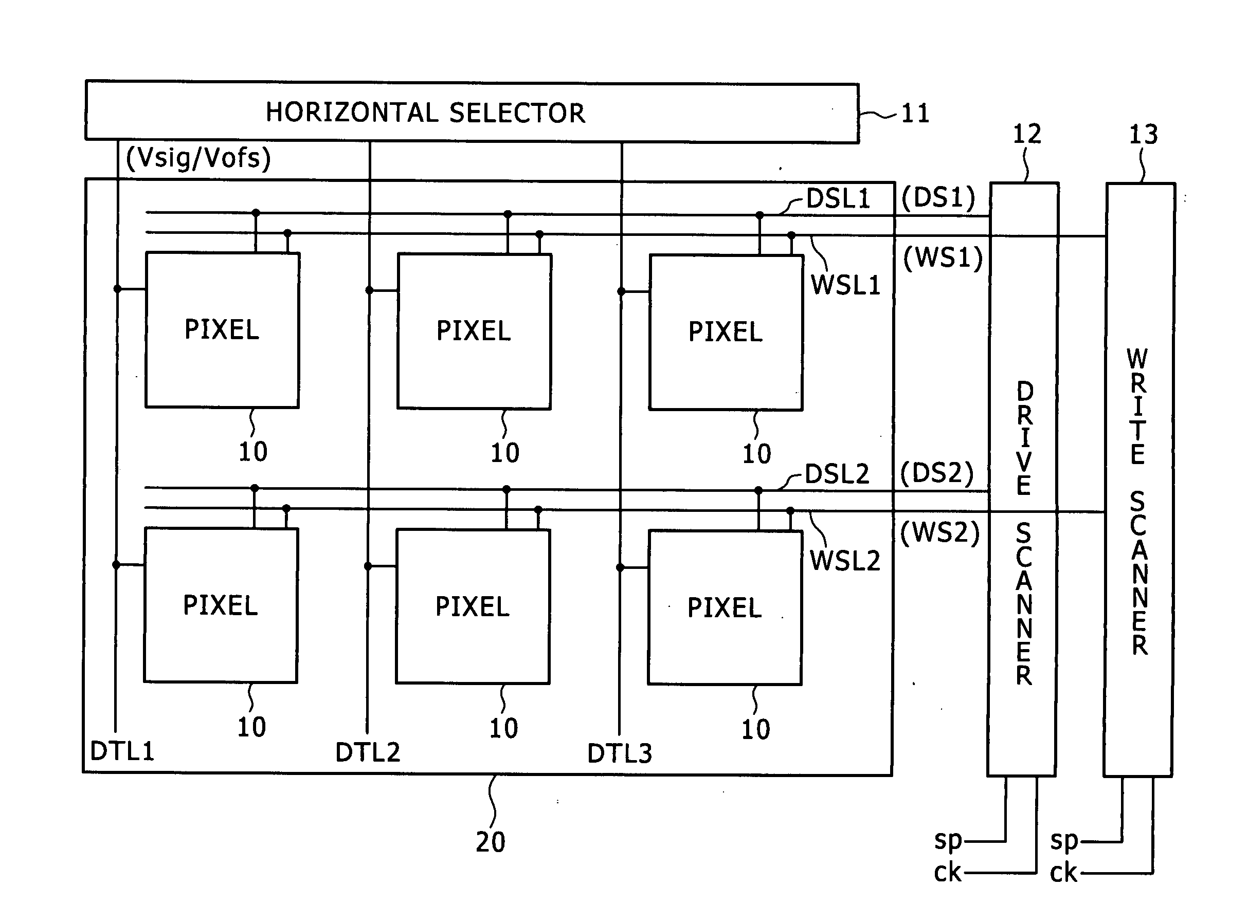
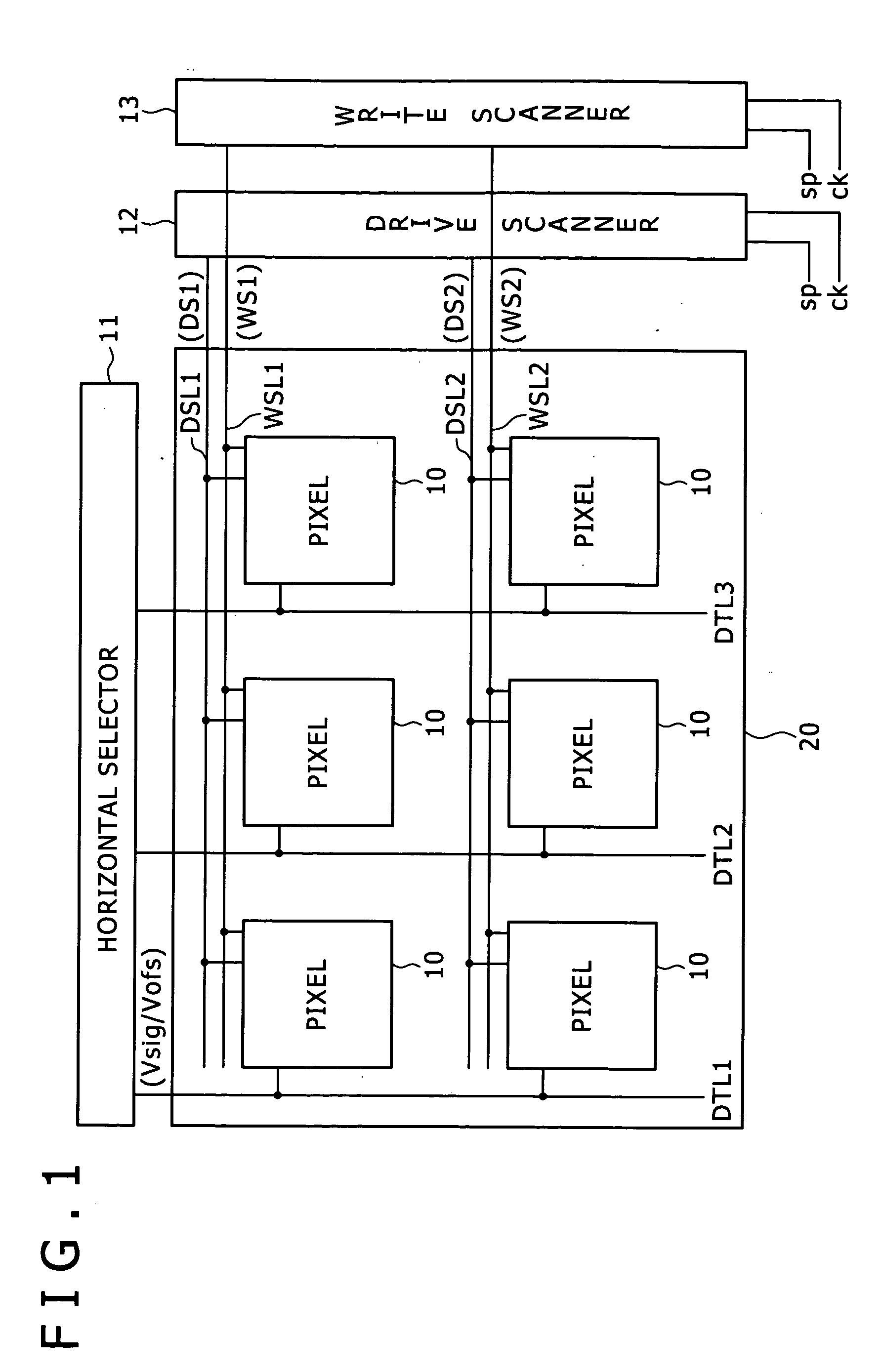
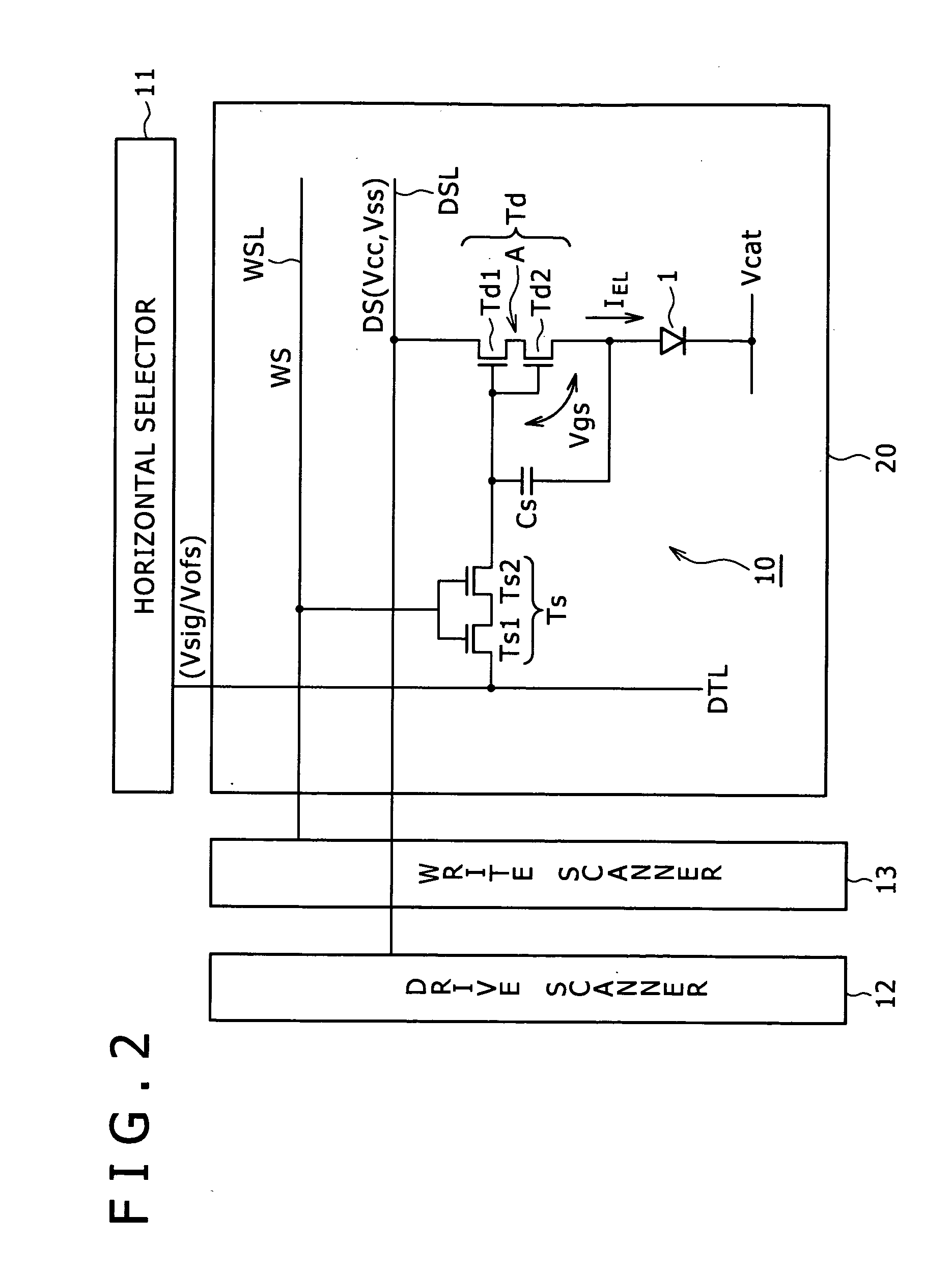
[0070]FIG. 1 shows a configuration of an organic EL display apparatus to which the present invention is applied.

[0071]Referring to FIG. 1, the organic EL display apparatus shown includes a plurality of pixel circuits 10 which use an organic EL element as a light emitting element thereof and are driven to emit light in accordance with an active matrix method.

[0072]In particular, the organic EL display apparatus includes a pixel array 20 including a large number of pixel circuits 10 arrayed in a matrix, that is, in m rows and n columns. It is to be noted that each of the pixel circuits ...


PUM


Abstract

A display apparatus includes: a pixel array including a plurality of pixel circuits disposed in a matrix and each including a light emitting element, a driving transistor for supplying current in response to a signal value applied between a gate and a source thereof to the light emitting element when a driving voltage is applied between a drain and the source thereof, and a holding capacitor connected between the gate and the source of the driving transistor for holding the input signal value, the driving transistor having a multi-gate structure wherein two or more transistors formed using an oxide semiconductor material are connected in series; and a light emission driving section.

Description

BACKGROUND OF THE INVENTION[0001]1. Field of the Invention[0002]This invention relates to a display apparatus having a pixel array including a plurality of pixel circuits disposed in a matrix and another display apparatus which uses an organic electroluminescence element, that is, an organic EL element.[0003]Japanese Patent Laid-Open Nos. 2003-255856 and 2003-271095 are known as related art documents to the inventor.[0004]2. Description of the Related Art[0005]In a display apparatus of the active matrix type wherein an organic electroluminescence (EL) light emitting element is used in a pixel, current to flow through a light emitting element in each pixel circuit is controlled by an active element, usually a thin film transistor (TFT), provided in the pixel circuit. In particular, since an organic EL element is a current light emitting element, a gradation of emitted light is obtained by controlling the amount of current to flow through the EL element.[0006]An example of a related a...

Claims


Application Information

Patent Timeline
IPC IPC(8): G09G5/10
CPCG09G3/3233G09G2300/0819G09G2300/0842H01L27/3262G09G2310/0251G09G2320/043G09G2320/045G09G2300/0866H10K59/1213
Inventor YAMAMOTO, TETSUROUCHINO, KATSUHIDESAGAWA, HIROSHI
Owner SONY CORP
Why Eureka
Try Eureka