LED module assemblies for displays

a technology for led modules and assemblies, applied in the direction of basic electric elements, electrical equipment, semiconductor devices, etc., can solve the problems of poor efficiency, difficult to maintain the height variation and flatness of black molded parts, and limited process, so as to increase the amount of light emitted from led chips, and improve the effect of light emitted

Active Publication Date: 2019-04-18
LUMENS
View PDF0 Cites 4 Cited by
  • Summary
  • Abstract
  • Description
  • Claims
  • Application Information

AI Technical Summary

Benefits of technology

[0024]In addition, a light absorbing material (for example, one including a black color material) is not present on the LED chips of the LED module assemblies according to the present invention, which is effective in increasing the amount of light emitted from the LED chips. Furthermore, a height variation is easier to maintain in the LED module assemblies of the present invention than in an LED module assembly including black molded parts formed by a squeezing process.
[0025]Moreover, according to the prior art, defective elements or parts are impossible to repair or correct after the formation of black molded parts by squeezing or transfer molding. In contrast, according to the present invention, only defective elements or parts can be repaired or corrected, resulting in high yield and low production cost.

Problems solved by technology

Further, the black molded parts 26 covering the upper portions of the LED chips decrease the amount of light emitted from the LED chips, resulting in poor efficiency.
However, this process is limited in that it is difficult to maintain the height variation and flatness of the black molded parts.

Method used


Image

  • LED module assemblies for displays
  • LED module assemblies for displays
  • LED module assemblies for displays

Examples


Embodiment Construction

[0034]Preferred embodiments of the present invention will now be described with reference to the accompanying drawings. The drawings and their description are intended to assist in understanding the present invention to those skilled in the art. Therefore, the drawings and the description should not be construed as limiting the scope of the present invention.

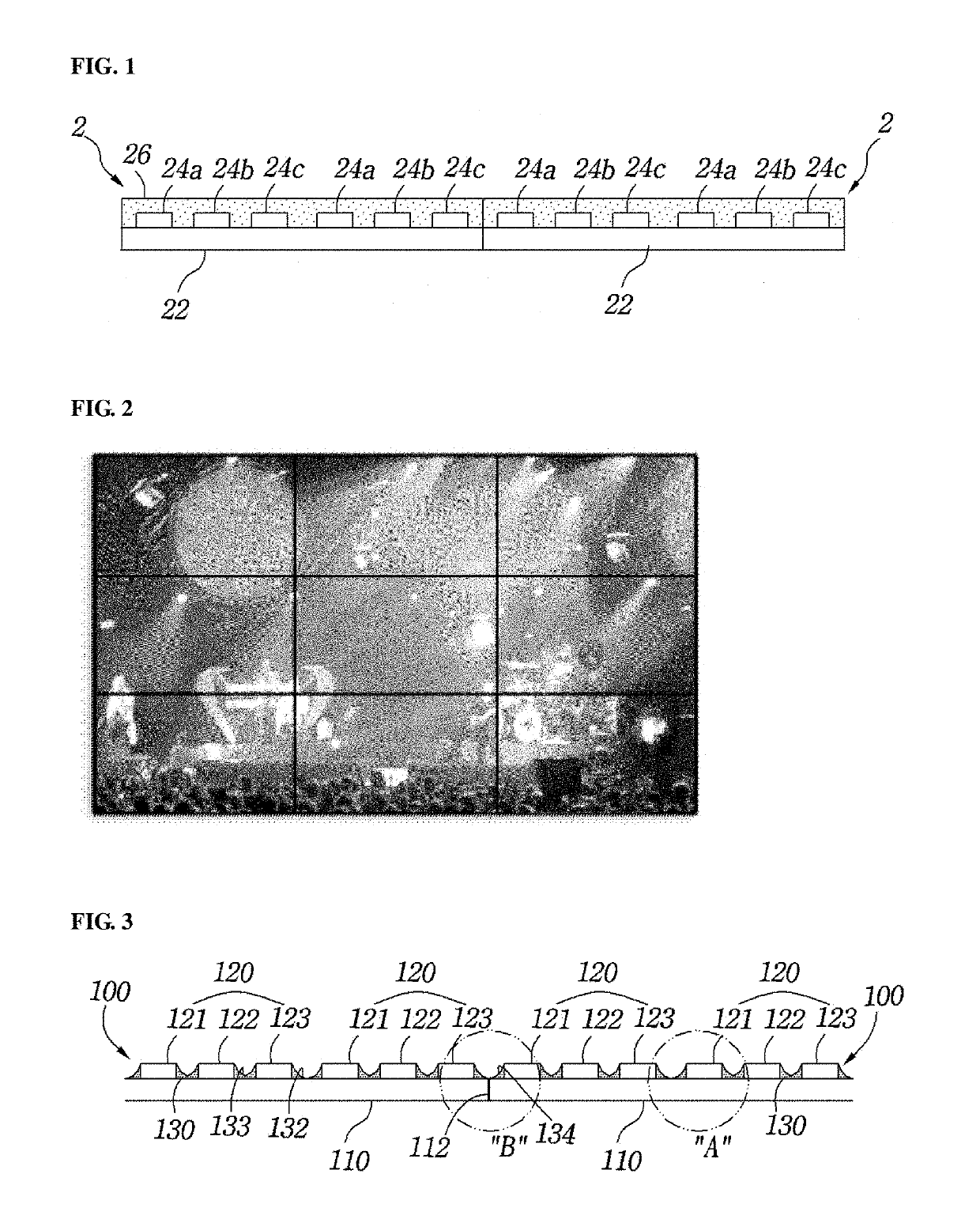
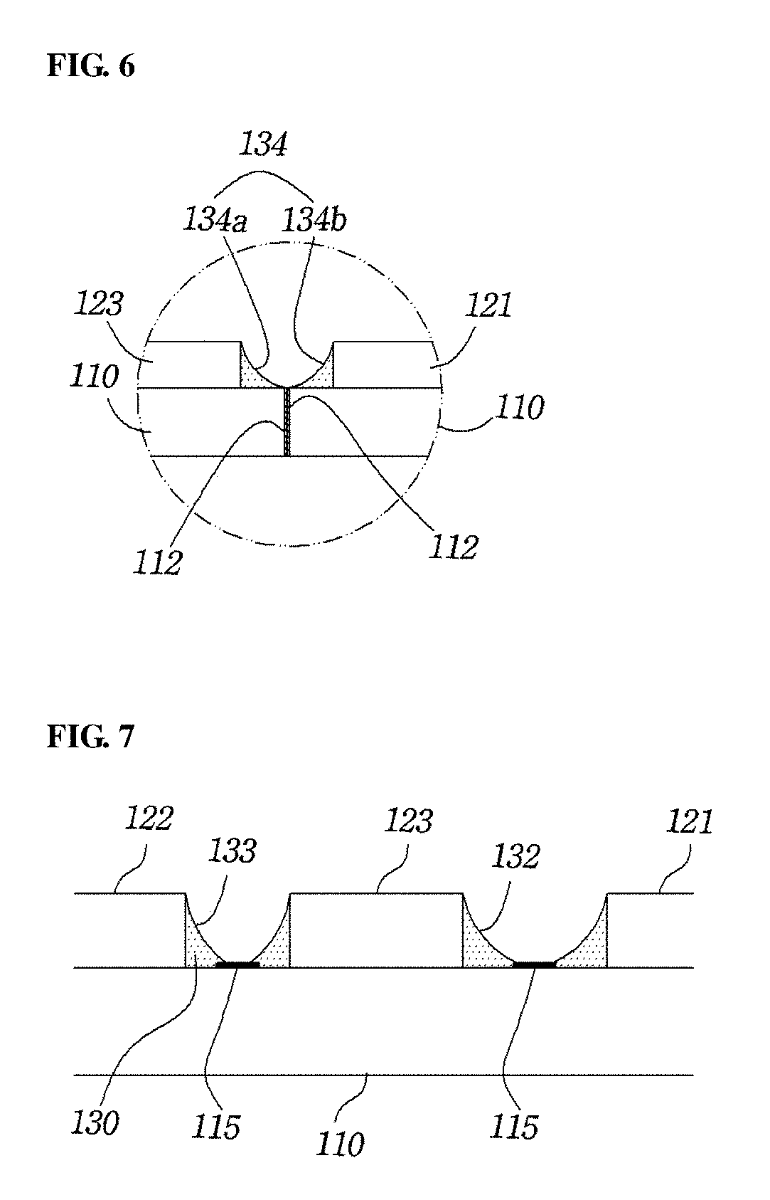
[0035]FIGS. 3 to 6 illustrate an LED module assembly according to one embodiment of the present invention.

[0036]As illustrated in FIGS. 3 to 6, the LED module assembly includes a plurality of LED modules 100 laterally connected to one another. The plurality of LED modules 100 include a first LED module 100, a second LED module, . . . , and an nth LED module. For convenience of illustration, the first LED module 100 and the second LED module 100 adjacent to each other are selected and denoted by the same reference numeral.

[0037]The LED module assembly includes a substrate including a first unit substrate 110 as a part of the firs...


PUM


Abstract

Disclosed is an LED module assembly for a display including a first LED module and a second LED module. The first LED module includes a first unit substrate, a plurality of LED chips mounted on the first unit substrate to form a plurality of pixels, and a first light absorbing layer formed on the first unit substrate. The second LED module includes a second unit substrate, a plurality of LED chips mounted on the second unit substrate to form a plurality of pixels, and a second light absorbing layer formed on the second unit substrate. The first unit substrate and the second unit substrate are laterally connected to each other. Each of the first light absorbing layer and the second light absorbing layer includes a plurality of valleys formed between the plurality of pixels. The first light absorbing layer includes a first inclined portion formed obliquely from the upper end edge of the interface between the first unit substrate and the second unit substrate to the upper portion of the side surface of each of the outer LED chips mounted on the first unit substrate. The second light absorbing layer includes a second inclined portion formed obliquely from the upper end edge of the interface between the first unit substrate and the second unit substrate to the upper portion of the side surface of each of the outer LED chips mounted on the second unit substrate. At least one of the plurality of valleys is formed by the first inclined portion and the second inclined portion meeting each other.

Description

BACKGROUND OF THE INVENTION1. Field of the Invention[0001]The present invention relates to LED module assemblies, and more specifically to LED module assemblies including LED modules laterally connected to one another such that color interference or diffuse reflection of light at the seams between the LED modules is prevented, achieving a seamless display.2. Description of the Related Art[0002]Techniques are already known wherein a plurality of LED modules are laterally connected to one another to construct an LED module assembly. Such a conventional LED module assembly is applied to an LED display.[0003]FIG. 1 illustrates a conventional LED module assembly including a plurality of LED modules 2 laterally connected to each other. As illustrated in FIG. 1, each of the plurality of LED modules 2 includes a unit substrate 22, a plurality of LED chips 24a, 24b, and 24c mounted on the unit substrate 22 to form a plurality of pixels, and a black molded part 26 formed on the unit substrate...

Claims


Application Information

Patent Timeline
Patent Type & Authority Applications(United States)
IPC IPC(8): H01L25/13H01L33/44H01L33/54
CPCH01L25/13H01L33/44H01L33/54H01L25/0753H01L33/58
Inventor MIN, CHUNKIKIM, KEUNOHNOH, HUIKYEONGCHO, KYUNGMIN
Owner LUMENS
Why Eureka
Try Eureka