Three-dimensional memory device and manufacturing method thereof

a technology of three-dimensional memory and manufacturing method, which is applied in the direction of semiconductor devices, semiconductor/solid-state device details, electrical devices, etc., can solve the problems of affecting the writing, reading and storing of data, and achieve the effect of increasing the data storage capacity

Active Publication Date: 2019-05-16
NUSTORAGE TECH CO LTD
View PDF0 Cites 7 Cited by
  • Summary
  • Abstract
  • Description
  • Claims
  • Application Information

AI Technical Summary

Benefits of technology

[0006]The present disclosure is to provide a three-dimensional memory device and a manufacturing method thereof, in which

Problems solved by technology

However, to replace the material having the perovskite structure with other ferroelectric materials, it is necessary to ensure that the ferroelectric characteristic of the ferro

Method used


Image

  • Three-dimensional memory device and manufacturing method thereof
  • Three-dimensional memory device and manufacturing method thereof
  • Three-dimensional memory device and manufacturing method thereof

Examples


Embodiment Construction

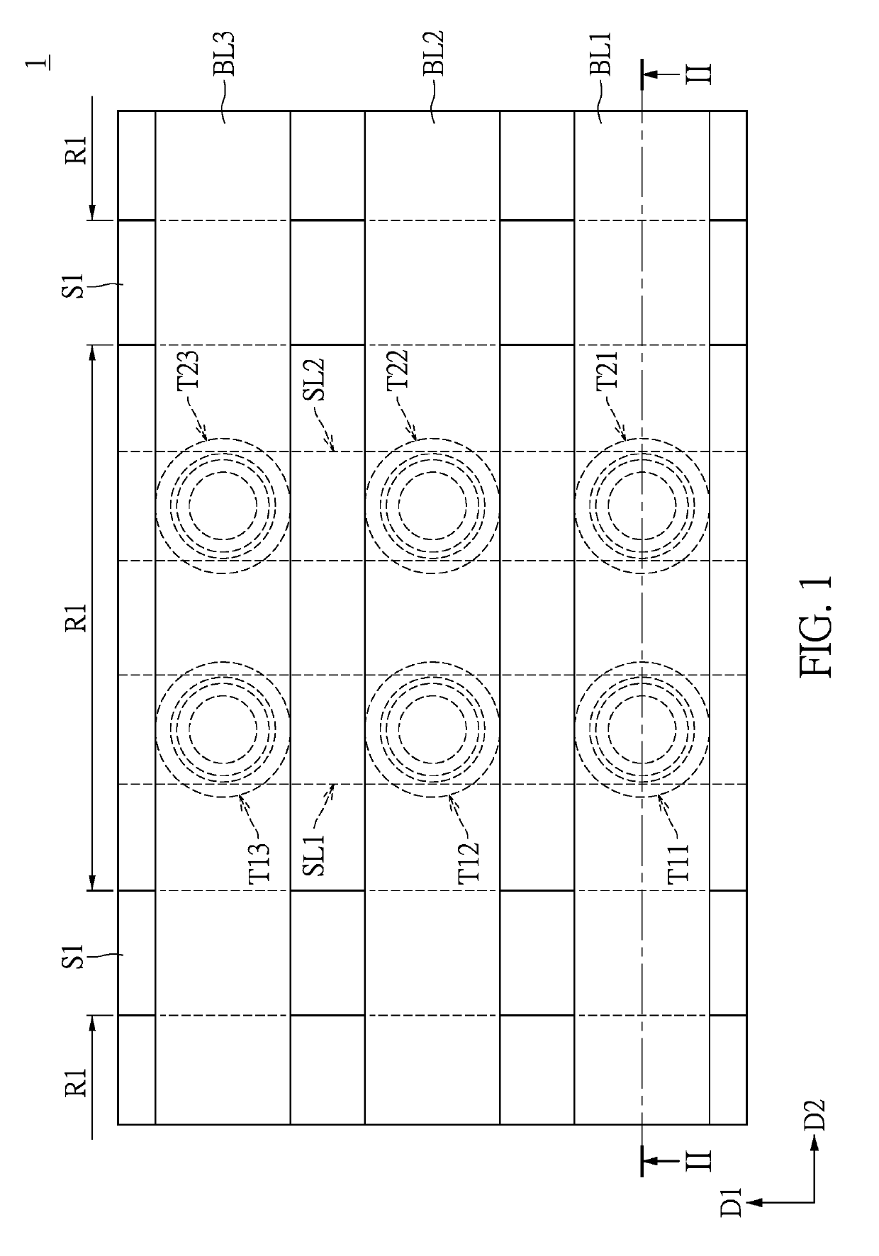
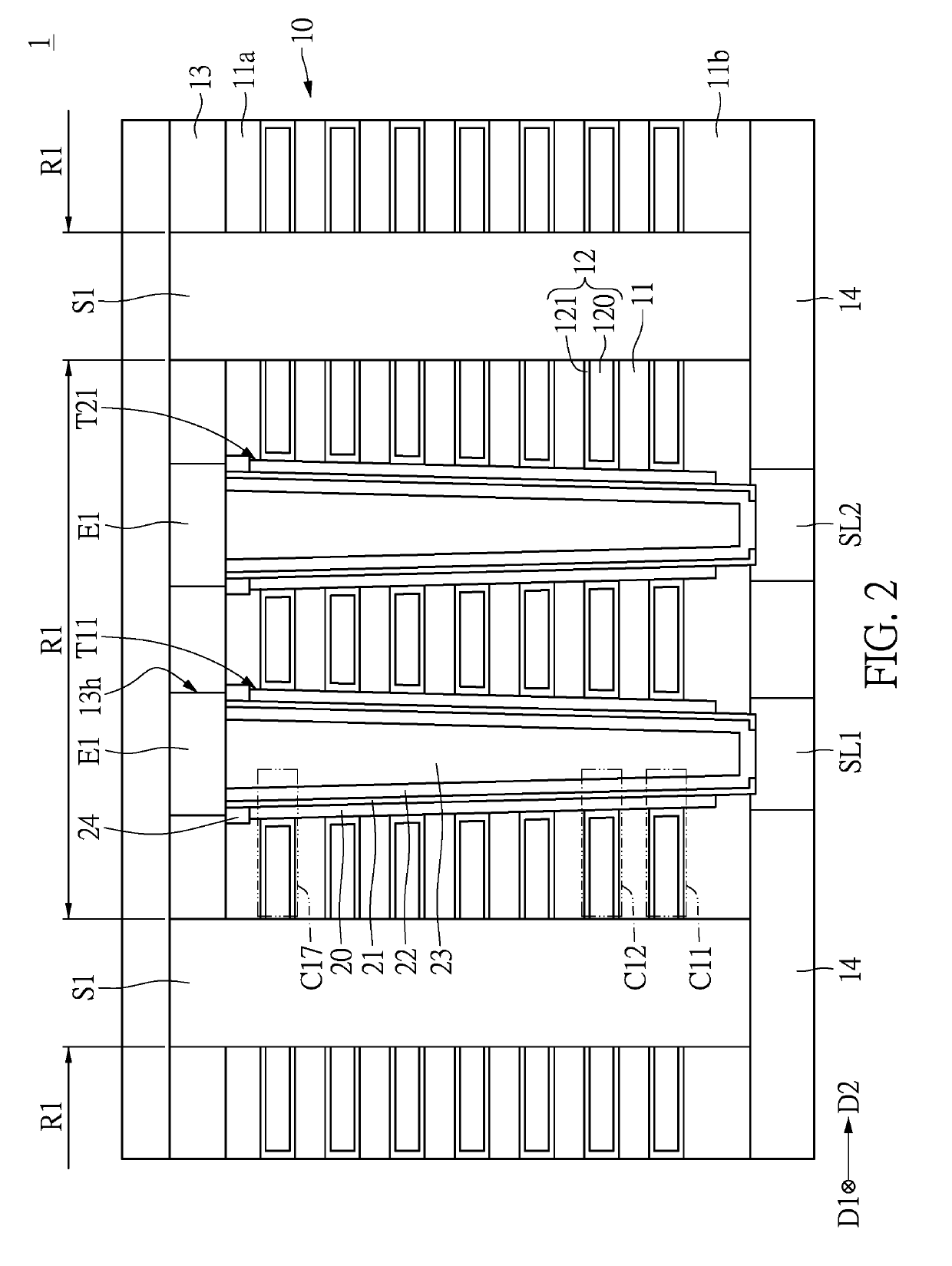
[0033]Referring to FIG. 1 to FIG. 2, FIG. 1 is a partial top view of a three-dimensional memory device according to an embodiment of the present disclosure, and FIG. 2 is a partial sectional view taken along line II-II of FIG. 1.

[0034]A three-dimensional memory device 1 in the embodiment of the present disclosure includes a plurality of bottom source lines SL1-SL2, a stacked structure 10, a plurality of bit lines BL1-BL3, and a plurality of pillar structures T11-T23.

[0035]The bottom source lines SL1-SL2 extend in a first horizontal direction D1 and are arranged in parallel. As shown in FIG. 1, the bottom source lines SL1-SL2 in the present embodiment are arranged in parallel along a second horizontal direction D2. Furthermore, the bottom source lines SL1-SL2 are disposed on another substrate (not shown in FIG. 1) and spaced from each other. In one embodiment, the three-dimensional memory device 1 further includes a plurality of insulating portions 14, and each of the insulating port...


PUM


Abstract

A three-dimensional memory device and a manufacturing method thereof are provided. The three-dimensional memory device includes a plurality of bottom source lines extending in a first horizontal direction, a stacked structure disposed on the bottom source lines, a plurality of bit lines extending in a second horizontal direction, and a plurality of pillar structures passing through the stacked structure. The stacked structure includes a plurality of composite structures spaced apart from one another and respectively located at different levels. The composite structures each include a gate conductive layer and a ferroelectric layer surrounding the gate conductive layer. Each of the pillar structures connected between the corresponding bit line and the corresponding bottom source line includes a barrier layer, a gate insulating layer, and a channel layer. The ferroelectric layer of each composite structure is insulated from the gate insulating layer of the pillar structure by the barrier layer.

Description

CROSS-REFERENCE TO RELATED PATENT APPLICATION[0001]This application also claim the priority benefit of a prior application serial no. CN 201711114898.5 filed Nov. 13, 2017. The entirety of the aforementioned patent applications is hereby incorporated by reference herein and made a part of this specification.FIELD OF THE DISCLOSURE[0002]The disclosure relates to a three-dimensional memory device and manufacturing method thereof in particular, to a vertical three-dimensional memory device and manufacturing method thereofBACKGROUND OF THE DISCLOSURE[0003]With recent evolvement of electronic devices, it has become a trend to develop memory devices having larger data storage capacity. In order to save data after the power is turned off, non-volatile memories, such as flash memory or ferroelectric random access memory (Fe-RAM), have received more attention. However, in order to process high-speed and large-capacity data, it is necessary to further develop a memory device which operates fa...

Claims


Application Information

Patent Timeline
IPC IPC(8): H01L27/11597H01L23/528H01L29/10H01L29/51H01L21/311H01L21/28H01L29/78H01L29/66H01L27/1159
CPCH01L27/11597H01L23/528H01L29/1037H01L29/516H01L29/517H01L21/31144H01L21/28291H01L29/78391H01L29/6684H01L27/1159H01L27/11587H01L29/40111H10B51/10H10B51/20H10B51/30
Inventor LIU, FU-CHOU
Owner NUSTORAGE TECH CO LTD
Why Eureka
Try Eureka