Communication filter for LTE band 41

a communication filter and lte band technology, applied in the field of electronic devices, can solve the problems of driving rf complexity in smartphones and limitations of conventional rf technology, and achieve the effects of low insertion loss, high interference rejection, and simple and cost-effectiv

Active Publication Date: 2019-06-13
AKOUSTIS INC
View PDF12 Cites 1 Cited by
  • Summary
  • Abstract
  • Description
  • Claims
  • Application Information

AI Technical Summary

Benefits of technology

[0007]In a specific example, the communication filter can be a bandpass RF filter characterized by the following: 50Ω input / output, no external matching requirement, low insertion loss, high interference rejection, −20° C. to +85° C. operation, +31 dBm absolute max input power, 2.0×1.6 mm footprint, 0.90 mm max height, RoHS 6 compliant, halogen free, and Tetrabromobisphenal A (TBBPA) free. This filter can be used in smartphones, tablets, Internet of things (IoT), and other mobile or portable communication devices. Those of ordinary skill in the art will recognize other variations, modifications, and alternatives.
[0008]One or more benefits are achieved over pre-existing techniques using the invention. In particular, the present device can be manufactured in a relatively simple and cost effective manner while using conventional materials and / or methods according to one of ordinary skill in the art. Using the present method, one can create a reliable single crystal based acoustic filter or resonator using multiple ways of three-dimensional stacking through a wafer level process. Such single crystal acoustic resonators enable high bandwidth-low loss filters in a miniature form factor, and such filters or resonators can be implemented in an RF filter device, an RF filter system, or the like. In an example, this communication filter can be a miniature filter configured for use in a 2496-2690 MHz wireless frequency spectrum. This filter can operate concurrently with adjacent 2.4 GHz bands including Wi-Fi, WLAN, Bluetooth, ISM, and the like. Depending upon the embodiment, one or more of these benefits may be achieved.

Problems solved by technology

Coexistence of new and legacy standards and thirst for higher data rate requirements is driving RF complexity in smartphones.
Unfortunately, limitations exist with conventional RF technology that is problematic, and may lead to drawbacks in the future.

Method used


Image

  • Communication filter for LTE band 41
  • Communication filter for LTE band 41
  • Communication filter for LTE band 41

Examples


Embodiment Construction

[0029]The present invention relates generally to electronic devices. More particularly, the present invention provides techniques related to bulk acoustic wave resonator devices, single crystal bulk acoustic wave resonator devices, single crystal filter and resonator devices, and the like. Merely by way of example, the invention has been applied to a single crystal resonator device for a communication device, mobile device, computing device, among others.

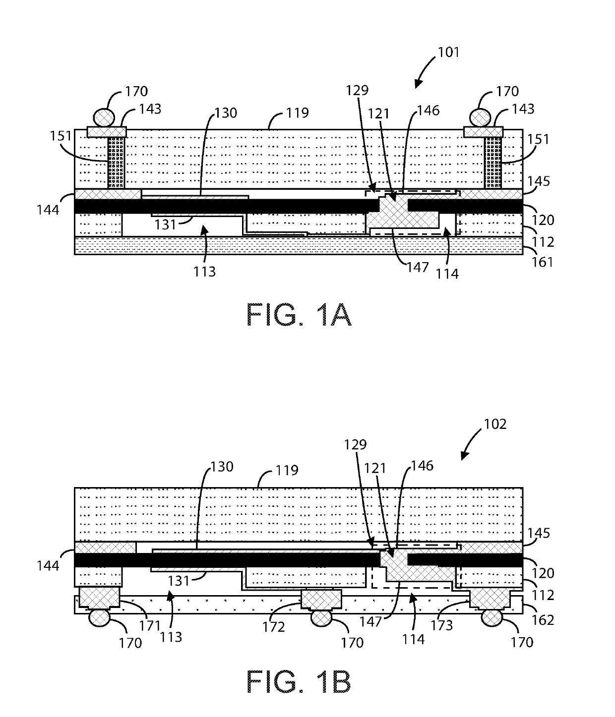
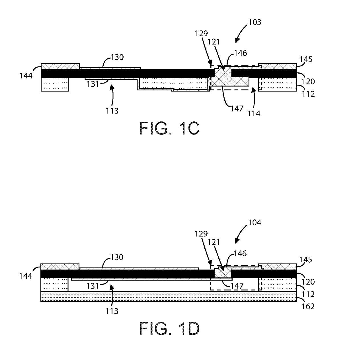
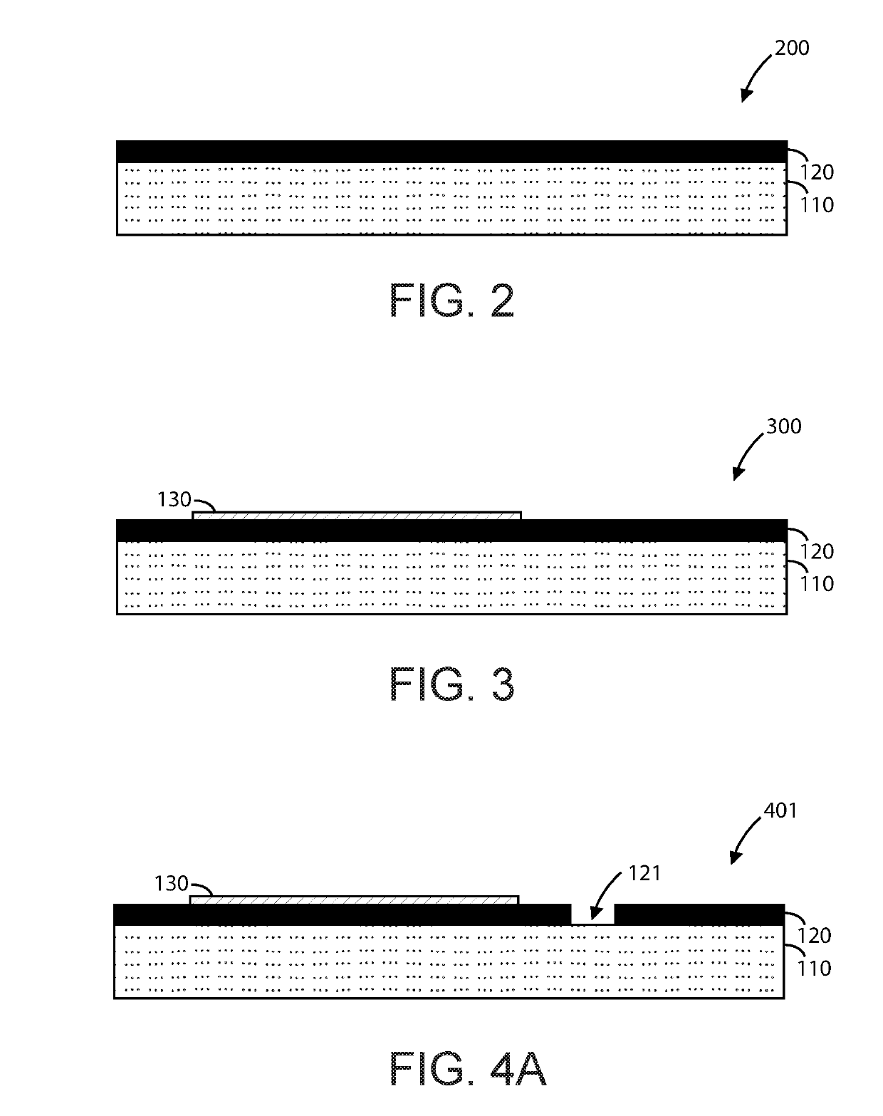
[0030]FIG. 1A is a simplified diagram illustrating an acoustic resonator device 101 having topside interconnections according to an example of the present invention. As shown, device 101 includes a transfer substrate 112 with an overlying single crystal piezoelectric layer 120, which has a micro-via 129. In a specific example, the piezoelectric layer is bonded to the transfer substrate using one or more dielectric layers containing silicon nitride, silicon oxide, or other adhesion materials. The micro-via 129 can include a topside m...


PUM

PropertyMeasurementUnit
diameteraaaaaaaaaa
diameteraaaaaaaaaa
diameteraaaaaaaaaa

Abstract

A communication system using a single crystal acoustic resonator device. The device includes a piezoelectric substrate with a piezoelectric layer formed overlying a transfer substrate. A topside metal electrode is formed overlying the substrate. A topside micro-trench is formed within the piezoelectric layer. A topside metal with a topside metal plug is formed within the topside micro-trench. First and second backside cavities are formed within the transfer substrate under the topside metal electrode. A backside metal electrode is formed under the transfer substrate, within the first backside cavity, and under the topside metal electrode. A backside metal plug is formed under the transfer substrate, within the second backside cavity, and under the topside micro-trench. The backside metal plug is connected to the topside metal plug and the backside metal electrode. The topside micro-trench, the topside metal plug, the second backside cavity, and the backside metal plug form a micro-via.

Description

CROSS-REFERENCES TO RELATED APPLICATIONS[0001]The present application is a continuation-in-part application of U.S. patent application Ser. No. 15 / 647,098, filed Jul. 11, 2017, which claims priority to U.S. Pat. App. No. 62 / 360,904, filed Jul. 11, 2016.BACKGROUND OF THE INVENTION[0002]The present invention relates generally to electronic devices. More particularly, the present invention provides techniques related to bulk acoustic wave resonator devices, single crystal bulk acoustic wave resonator devices, single crystal filter and resonator devices, and the like. Merely by way of example, the invention has been applied to a single crystal resonator device for a communication device, mobile device, computing device, among others.[0003]Mobile telecommunication devices have been successfully deployed world-wide. Over a billion mobile devices, including cell phones and smartphones, were manufactured in a single year and unit volume continues to increase year-over-year. With ramp of 4G / ...

Claims


Application Information

Patent Timeline
Patent Type & Authority Applications(United States)
IPC IPC(8): H03H9/17H03H9/70H03H9/56H03H3/02
CPCH03H9/172H03H9/706H03H9/564H03H3/02H03H2003/023H03H9/0523H03H9/1007H03H9/174H03H2003/021H03H9/105H03H9/173H03H9/566
Inventor GIBB, SHAWN R.VETURY, RAMAKRISHNASHEALY, JEFFREY B.BOOMGARDEN, MARK D.LEWIS, MICHAEL P.FELDMAN, ALEXANDER Y.
Owner AKOUSTIS INC
Why Eureka
Try Eureka