Aluminum nitride thin film, composite film containing the same and piezoelectric thin film resonator using the same

a technology of aluminum nitride and composite film, which is applied in the field of piezoelectric thin film, can solve the problems that the piezoelectric thin film resonator or piezoelectric thin film filter that exhibits sufficient performance at a gigahertz band has not been achieved, and achieves excellent piezoelectric thin film, improve remarkably characteristics, and high crystallinity

Active Publication Date: 2009-01-27
MEMS SOLUTIONS INC
View PDF8 Cites 65 Cited by
  • Summary
  • Abstract
  • Description
  • Claims
  • Application Information

AI Technical Summary

Benefits of technology

[0011]Hence, the present invention has an object of providing a piezoelectric thin film resonator which attains high electromechanical coupling coefficient, excellent acoustic quality factors (Q-value) of both resonance and anti-resonance, excellent frequency temperature characteristics, and remarkably higher performance in characteristics such as an excellent bandwidth, low insertion loss, and the like in comparison with conventional resonators, while making use of a merit of an AlN thin film allowing high propagation speed of acoustic wave.
[0012]The present inventors eagerly studied and discussed effects of material and crystallinity of a lower electrode on crystallinity and orientation of an aluminum nitride thin film which greatly influence resonance characteristics of an FBAR or SBAR. As a result, the present inventors found out that a c-axis oriented aluminum nitride thin film having high crystallinity and high crystal orientation is obtained by using as the lower electrode a metal thin film containing ruthenium as a major component and by forming an aluminum nitride thin film on the metal thin film. On the c-axis oriented aluminum nitride thin film, a full-width half maximum (FWHM) of a rocking curve of a (0002) diffraction peak is 2.0° or less. The inventors further found out that by manufacturing the metal thin film having a particular crystal phase and a particular crystallinity degree, a c-axis oriented aluminum nitride thin film having much higher orientation and crystallinity can be obtained with a full-width half maximum (FWHM) of a rocking curve of 0.8 to 1.6°. Further, the inventors found that a high performance FBAR or SBAR which exhibits excellent band width characteristics and excellent frequency temperature characteristics with low insertion loss can be achieved by using the c-axis oriented aluminum nitride thin film mentioned above. The present invention has thus been approached.
[0041]Further, according to the present invention, there is provided a piezoelectric thin film device having the above piezoelectric thin film resonator. The piezoelectric thin film resonator includes a stacked piezoelectric thin film resonator. The piezoelectric thin film device is not limited to but may be, for example, a VCO (Voltage Control Oscillator), a filter, a duplexer, or the like which comprises the piezoelectric thin film resonator or stacked piezoelectric thin film resonator. These piezoelectric thin film devices are capable of improving remarkably characteristics at a high frequency not lower than 1 GHz.
[0042]According to the present invention, a lower electrode is constituted using a metal thin film including a layer containing ruthenium as a major component. Crystallinity and crystal orientation and of a c-axis oriented aluminum nitride thin film formed on the lower electrode is improved remarkably by specifying a crystal orientation and thickness of the lower electrode, and structure of the lower electrode and an insulating layer optionally used. Thus, a c-axis oriented aluminum nitride thin film can be formed with high crystallinity and orientation whose full-width half maximum (FWHM) of a rocking curve of a (0002) diffraction peak is 2.0° or less. Further, an excellent piezoelectric thin film can be formed by setting a tapered angle of an end face of the lower electrode within a predetermined range. As a result, it is possible to improve an acoustic quality factor (Q value) of an anti-resonance peak in an impedance characteristic, which is a problem in a conventional electrode structure. There can be provided accordingly a piezoelectric thin film resonator which has an excellent electromechanical coupling coefficient kt2 and an excellent acoustic quality factor (Q value). Therefore, performance of a VCO (Voltage Control Oscillator), a filter, and a duplexer constituted by using the piezoelectric thin film resonator can be improved at a high frequency of 1 GHz or more.

Problems solved by technology

However, a piezoelectric thin film resonator or piezoelectric thin film filter that exhibits sufficient performance at a gigahertz band has not been achieved.

Method used


Image

  • Aluminum nitride thin film, composite film containing the same and piezoelectric thin film resonator using the same
  • Aluminum nitride thin film, composite film containing the same and piezoelectric thin film resonator using the same
  • Aluminum nitride thin film, composite film containing the same and piezoelectric thin film resonator using the same

Examples


example 1

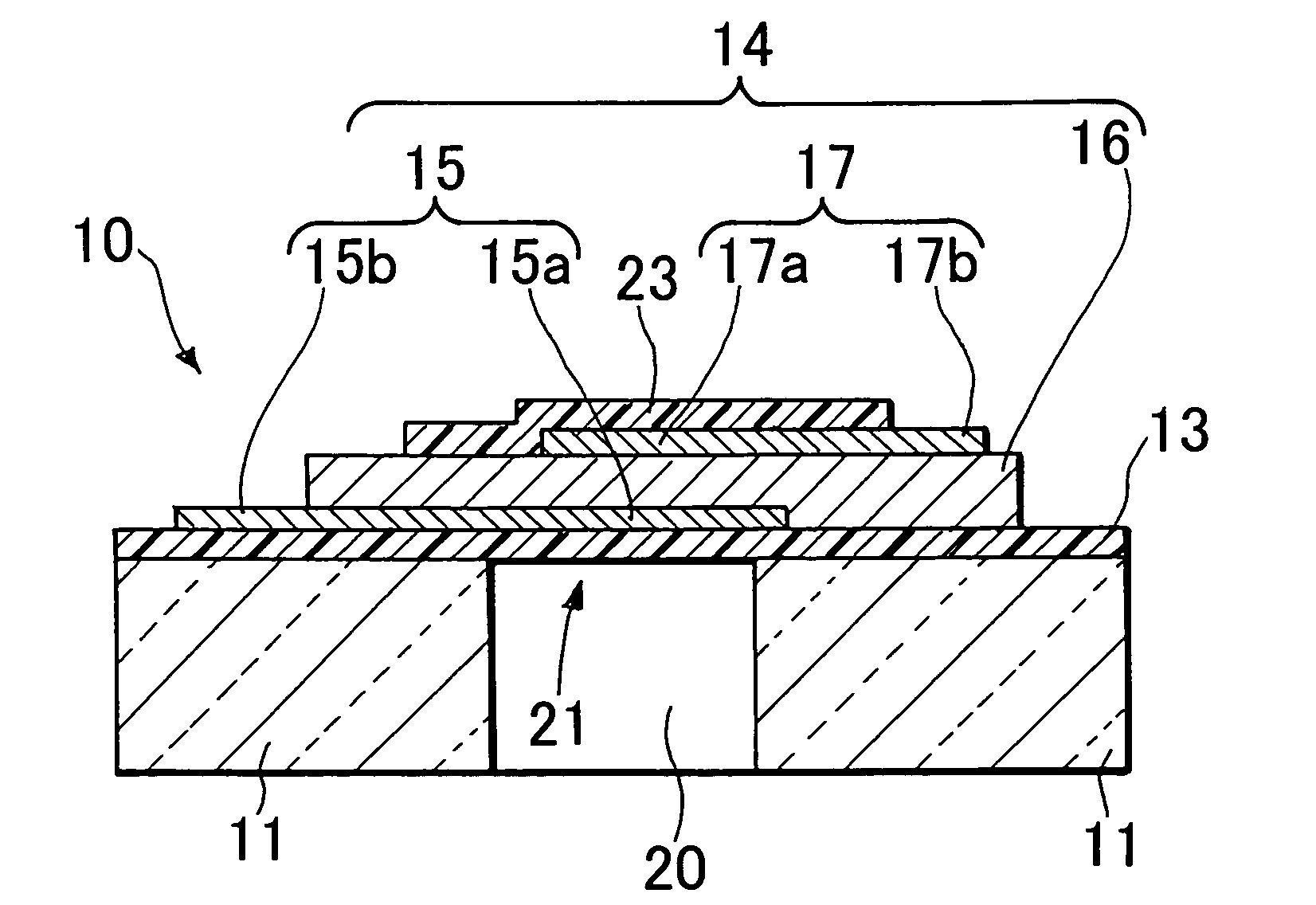
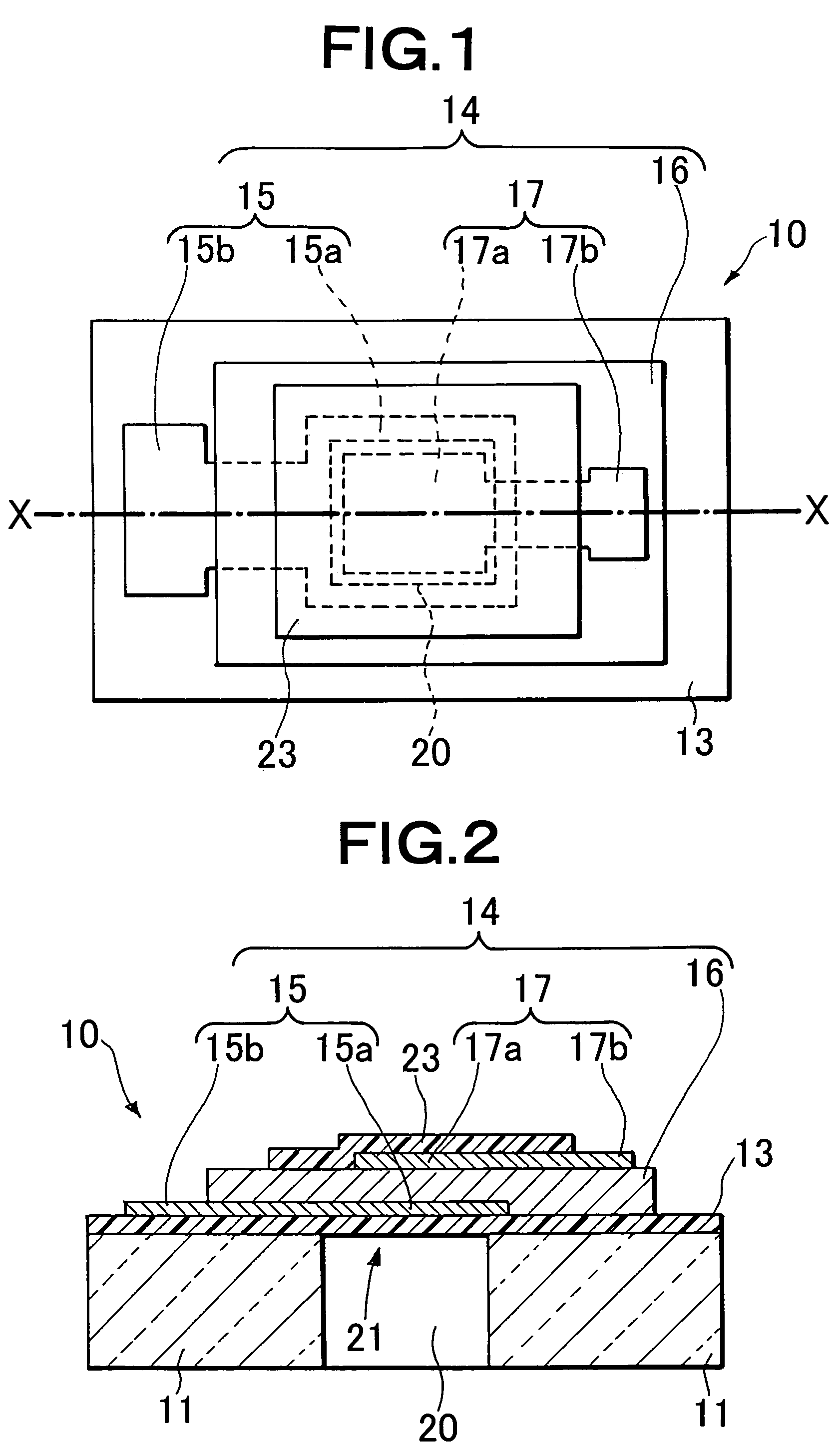
[0090]In this example, a piezoelectric thin film resonator having a structure shown in FIGS. 1 and 2 was manufactured as follows.

[0091]Specifically, an SiO2 layer having a thickness of 1,000 nm was formed by a thermal oxidation method on each of both surfaces of a (100) Si substrate having a thickness of 300 μm. Thereafter, a mask pattern corresponding to the shape of the via hole 20 was formed on a second surface (lower surface) side, and a part of the SiO2 layer which corresponds to the pattern was etched and removed. Simultaneously, all the SiO2 layer in a first surface (upper surface) side was etched and removed. Next, an Al2O3 thin film having a thickness of 220 nm was formed on the first surface side by a reactive sputtering method. On a first surface of this Si substrate, a Mo thin film having a thickness of 90 nm and an Ru thin film having a thickness of 100 nm were deposited orderly by a DC magnetron sputtering method, to form a lower electrode layer. Further, patterning wa...

example 2

[0093]In this example, a piezoelectric thin film resonator having the structure shown in FIGS. 1 and 2 was manufactured as follows. Specifically, the piezoelectric thin film resonator shown in FIGS. 1 and 2 was manufactured by similar methods to those in Example 1 except that the materials and thicknesses of the lower and upper insulating layers, the forming conditions and thickness of the Ru / Mo-layered lower electrode, and the material and thickness of the upper electrode were changed. Tables 1 and 2 show the material and thickness of each layer at the vibration portion, and a full-width half maximum (FWHM) of a rocking curve of the Ru / Mo-layered lower electrode. Table 3 shows a full-width half maximum (FWHM) of a rocking curve of the AlN thin film.

[0094]Further, a GSG micro prober manufactured by Cascade Microtech Inc. and a network analyzer were used to measure an impedance characteristic between the electrode terminals 15b and 17b of the piezoelectric thin film resonator. In add...

example 3

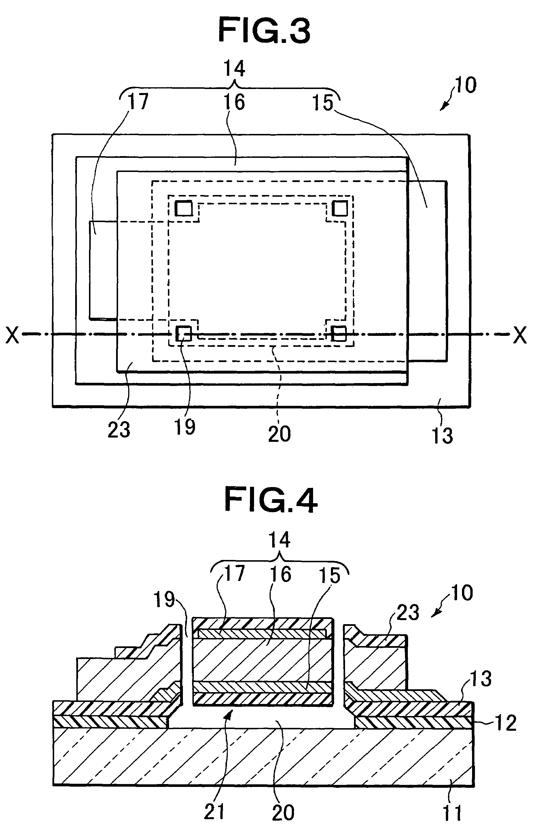
[0095]In this example, a piezoelectric thin film resonator having the structure shown in FIGS. 3 and 4 was manufactured as follows. Specifically, an SiO2 layer having a thickness of 1,500 nm was formed by a thermal oxidation method on each of both surfaces of an Si substrate having a thickness of 625 μm. Thereafter, a Ti thin film having a thickness of 50 nm to become a sacrifice layer was deposited on a first surface (upper surface) of the Si substrate, and a pattern was formed into a desired air bridge shape by photolithography. Next, an AlN thin film having a thickness of 100 nm was formed on the first surface side by a reactive sputtering method. On the first surface of this Si substrate, a Mo thin film and a Ru thin film which had thicknesses shown in Table 1 were deposited orderly by a DC magnetron sputtering method to form a lower electrode layer, which was further patterned by photolithography. In the pattern formation, resist was exposed to intentionally defocused ultraviol...


PUM

PropertyMeasurementUnit
thickness d2aaaaaaaaaa

Abstract

A piezoelectric thin film resonator has a substrate and a piezoelectric layered structure including a lower electrode, piezoelectric aluminum nitride thin film with c-axis orientation and upper electrode formed on the substrate in this order. The lower electrode are made of a metal thin film including a layer containing ruthenium as a major component having a full-width half maximum (FWHM) of a rocking curve of a (0002) diffraction peak of ruthenium of 3.0° or less. The piezoelectric aluminum nitride thin film formed on the lower electrode has a full-width half maximum (FWHM) of a rocking curve of a (0002) diffraction peak of 2.0° or less.

Description

[0001]This application claims priority benefits from Japanese Patent Application No. 2005-297192 filed Oct. 12, 2005.BACKGROUND OF THE INVENTION[0002]1. Field of the Invention[0003]The present invention relates to a piezoelectric thin film used in wide fields and a device to which the piezoelectric thin film is applied, such as a thin film resonator, a thin film VCO (Voltage Control Oscillator), a thin film filter, a duplexer, or various sensors for use in a mobile communication device or the like.[0004]2. Description of the Related Art[0005]Devices using piezoelectric phenomena are used in a wide range of fields. While downsizing and power saving of mobile devices progress, use of SAW (Surface Acoustic Wave) devices as RF and IF filters has been expanding. SAW filters have improved in designs and production techniques to meet users' demands for strict specifications. However, improvements in characteristics of SAW filters are approaching limits as used frequencies rise higher. This...

Claims


Application Information

Patent Timeline
Patent Type & Authority Patents(United States)
IPC IPC(8): H03H9/125H01L41/083H01L41/09H01L41/18H01L41/22H01L41/319H03H9/17
CPCH03H3/02H03H9/02031H03H9/13H03H9/173H03H9/174H03H9/585H03H2003/021H03H2003/023H10N30/877
Inventor YAMADA, TETSUONAGAO, KEIGOMASUI, EIJI
Owner MEMS SOLUTIONS INC
Why Eureka
Try Eureka