Method for manufacturing a vibrating MEMS circuit

a technology of microelectromechanical systems and manufacturing methods, applied in piezoelectric/electrostrictive/magnetostrictive devices, piezoelectric/electrostrictive device details, device details, etc., can solve the problems of poor frequency stability of deposited thin films of fposr, difficult control, limiting or expensive, etc., to achieve precise sizes and shapes, increase the electromechanical coupling coefficient, and reduce the temperature coefficient of frequency

Active Publication Date: 2016-06-14
QORVO US INC
View PDF42 Cites 76 Cited by
  • Summary
  • Abstract
  • Description
  • Claims
  • Application Information

AI Technical Summary

Benefits of technology

[0007]The present invention relates to a micro-electro-mechanical systems (MEMS) vibrating structure supported by a MEMS anchor system, and includes a single-crystal piezoelectric thin-film layer that has a specific non-standard crystal orientation, which may be selected to increase an electromechanical coupling coefficient, decrease a temperature coefficient of frequency, or both. The MEMS vibrating structure may have dominant lateral vibrations or dominant thickness vibrations. The single-crystal piezoelectric thin-film layer may include Lithium Tantalate or Lithium Niobate, and may provide MEMS vibrating structures with precise sizes and shapes, which may provide high accuracy and enable fabrication of multiple resonators having different resonant frequencies on a single substrate.
[0008]Since the MEMS vibrating structure is formed from a single-crystal material and uses mechanically efficient MEMS construction, the MEMS vibrating structure may be high-Q, low loss, stable, have a low temperature coefficient of frequency, have a high electromechanical coupling coefficient, have high repeatability, and have a low motional impedance.

Problems solved by technology

Therefore, a resonant frequency of the FBAR may be dependent upon the thickness of a deposited Aluminum Nitride layer, which may be difficult to control.
Additionally, a separate Aluminum Nitride layer may be needed for an additional FBAR having a different resonant frequency, which may be limiting or expensive.
However, the deposited thin-film of the FPOSR may have poor frequency stability, high losses, and may have a relatively low electromechanical coupling coefficient due to loading by a substrate layer.

Method used


Image

  • Method for manufacturing a vibrating MEMS circuit
  • Method for manufacturing a vibrating MEMS circuit
  • Method for manufacturing a vibrating MEMS circuit

Examples


first embodiment

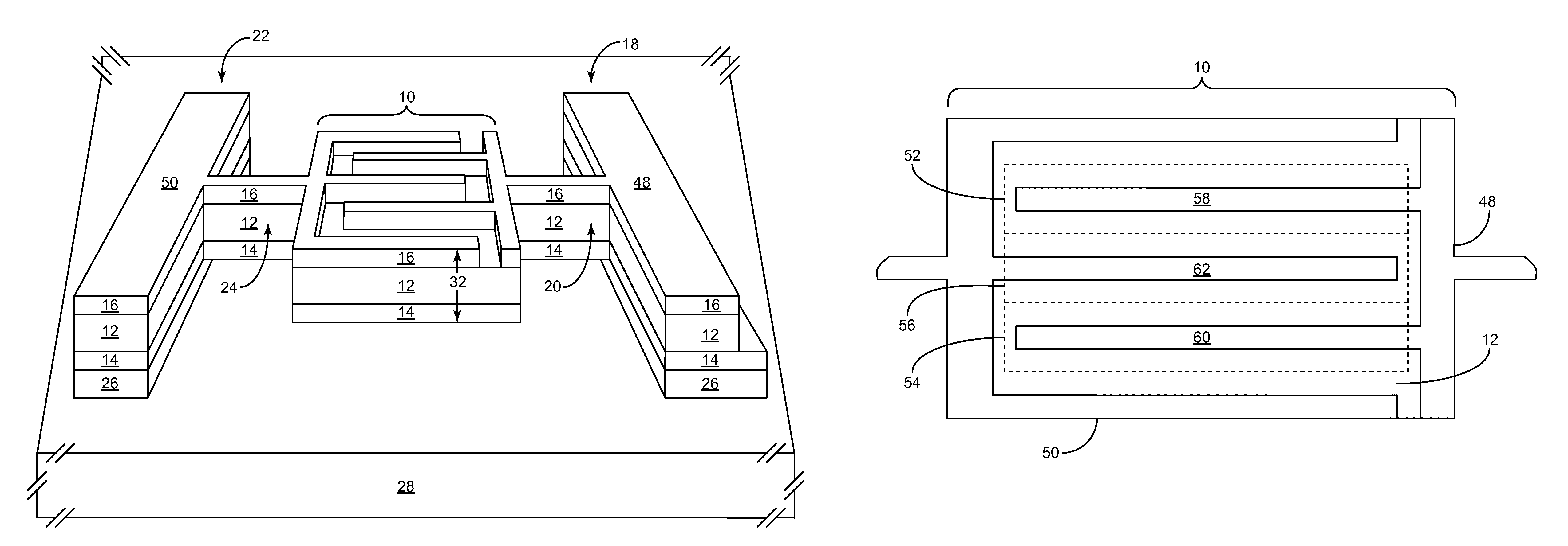
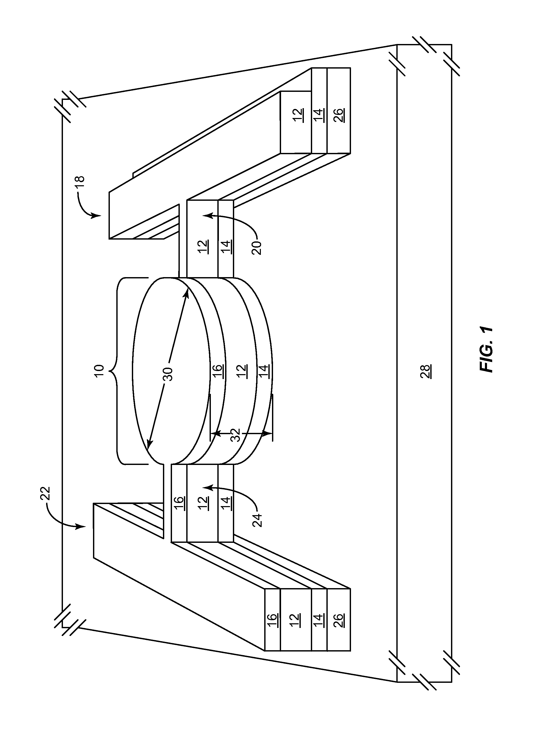
[0037]One vibrational characteristic is resonant frequency. The single-crystal piezoelectric thin-film layer 12 in the MEMS vibrating structure 10 may have at least one resonant region (not shown) having at least one resonant frequency. Another vibrational characteristic is the electromechanical coupling coefficient, which relates the mechanical characteristics to the electrical characteristics of the MEMS vibrating structure 10, and may be useful for radio frequency (RF) filter applications or high-Q RF circuits. An additional vibrational characteristic is the dominant mode of vibration. In the MEMS vibrating structure 10, the shape of the MEMS vibrating structure 10 is a disk having an outer diameter 30 and a thickness 32, as illustrated in FIG. 1. The dominant mode of vibration is a contour mode of vibration, which is one form of lateral vibration, wherein the outer diameter 30 varies as the MEMS vibrating structure 10 vibrates.

[0038]In a second embodiment of the MEMS vibrating s...

fourth embodiment

[0039]In the MEMS vibrating structure 10, the shape of the MEMS vibrating structure 10 is a circular ring having the outer diameter 30, an inner diameter 38, and the thickness 32, as illustrated in FIG. 3. The dominant mode of vibration is a contour mode of vibration, which is one form of lateral vibration, wherein the outer diameter 30, the inner diameter 38, or both, vary as the MEMS vibrating structure 10 vibrates.

[0040]In a fifth embodiment of the MEMS vibrating structure 10, the shape of the MEMS vibrating structure 10 is the circular ring, as illustrated in FIG. 3. The dominant mode of vibration is a thickness-extensional mode of vibration, which is one form of thickness vibration, wherein the thickness 32 varies as the MEMS vibrating structure 10 vibrates. In a sixth embodiment of the MEMS vibrating structure 10, the shape of the MEMS vibrating structure 10 is the circular ring, as illustrated in FIG. 3. The dominant mode of vibration is a thickness-shear mode of vibration, w...


PUM

PropertyMeasurementUnit
angleaaaaaaaaaa
angleaaaaaaaaaa
angleaaaaaaaaaa

Abstract

A method for making a micro-electro-mechanical systems (MEMS) vibrating structure is disclosed. The MEMS is supported by a MEMS anchor system and includes a single-crystal piezoelectric thin-film layer that has a specific non-standard crystal orientation, which may be selected to increase an electromechanical coupling coefficient, decrease a temperature coefficient of frequency, or both. The MEMS vibrating structure may have dominant lateral vibrations or dominant thickness vibrations. The single-crystal piezoelectric thin-film layer may include Lithium Tantalate or Lithium Niobate, and may provide MEMS vibrating structures with precise sizes and shapes, which may provide high accuracy and enable fabrication of multiple resonators having different resonant frequencies on a single substrate.

Description

[0001]This application claims the benefit of provisional patent application Ser. No. 60 / 969,314, filed Aug. 31, 2007, the disclosure of which is hereby incorporated herein by reference in its entirety.FIELD OF THE INVENTION[0002]Embodiments of the present invention relate to micro-electro-mechanical systems (MEMS) vibrating structures, such as MEMS sensors, MEMS resonators, MEMS oscillators, or MEMS filters, which may be used in radio frequency (RF) communications systems.BACKGROUND OF THE INVENTION[0003]Resonators are devices that are often used in radio frequency (RF) circuitry in frequency reference circuits and filter circuits. Generally, resonators need to be high-Q, low loss, stable, have a low temperature coefficient of frequency, have high repeatability, have high accuracy, and have a low motional impedance. Additionally, RF circuits often require multiple resonators having different resonant frequencies. In some applications, such as RF filters, resonators need to have a wi...

Claims


Application Information

Patent Timeline
Patent Type & Authority Patents(United States)
IPC IPC(8): H03H3/02H01L41/047H03H9/05H03H9/02H01L41/04H01L41/053H01L41/311H01L41/29H03H9/15
CPCH03H9/0542H01L41/29H01L41/047H03H9/02062H01L41/311H03H9/0547H03H3/02H03H9/0207H01L41/053Y10T29/49005Y10T29/49155Y10T29/42H03H2009/02283H03H2009/02299H03H2009/155Y10T29/49147H03H3/0076H03H9/02015H03H9/17H10N30/06H10N30/071H10N30/87H10N30/88
Inventor LI, SHENG-SHIANLEE, SEUNGBAEBHATTACHARJEE, KUSHAL
Owner QORVO US INC
Why Eureka
Try Eureka