Low temperature coefficient field effect transistors and design and fabrication methods

Inactive Publication Date: 2009-05-28
THUNDERBIRD TECH
View PDF22 Cites 6 Cited by
  • Summary
  • Abstract
  • Description
  • Claims
  • Application Information

AI Technical Summary

Benefits of technology

[0005]An accumulation mode field effect transistor according to various embodiments of the present invention includes a substrate, an insulated gate on the substrate, source and drain regions on the substrate on opposite sides of the insulated gate, a channel region that is doped a first conductivity type at a first doping concentration, and that extends into the substrate beneath the insulated gate to a channel region depth, and a counter-doped region (for example, a portion of the substrate, a tub in the substrate or a well in the substrate) beneath the channel region that is doped a second conductivity type at a second doping concentration to define a semiconductor junction therebetween at the channel region depth. According to various embodiments, the first doping concentration, the second doping concentration and the channel region depth are selected to counterbalance a threshold voltage change of the accumulation mode field effect transistor as a function of temperature against a majority carrier mobility change of the accumulation mode field effect transistor as a function of temperature, so as to provide a low temperature coefficient accumulation mode field effect transistor.
[0006]In other embodiments, the first doping concentration, the second doping concent

Problems solved by technology

These short channel devices may make it increasingly difficult to design high performance circuits and integrated circuits

Method used


Image

  • Low temperature coefficient field effect transistors and design and fabrication methods
  • Low temperature coefficient field effect transistors and design and fabrication methods
  • Low temperature coefficient field effect transistors and design and fabrication methods

Examples


Embodiment Construction

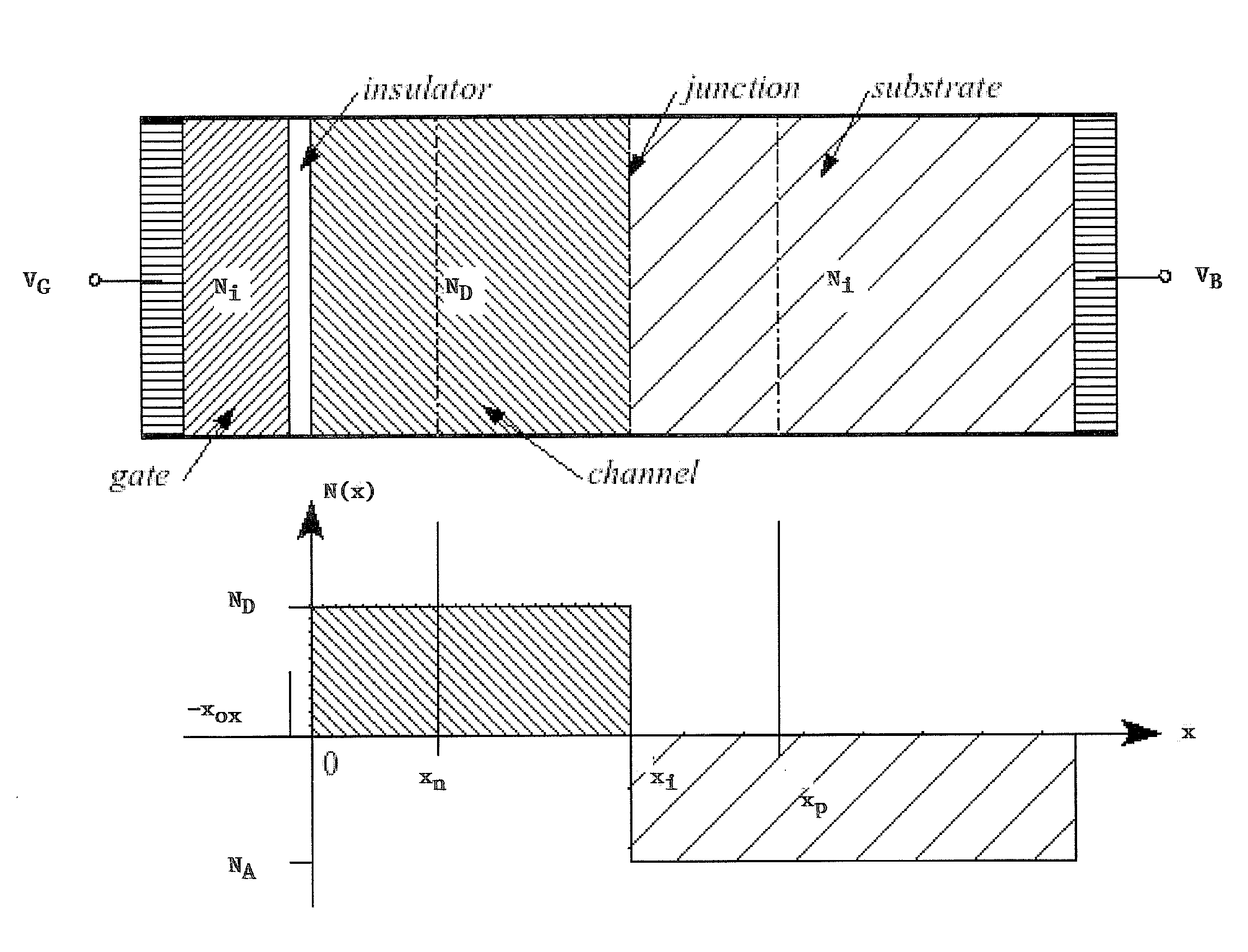
[0016]It has been discovered that accumulation mode field effect transistors may be designed and built with extremely low temperature coefficients in drive current, with gate voltage and drain voltage equal to the supply voltage. A reason for this unpredictable result is that counter-doped devices belong to a class of MOSFETs which may be considered accumulation, rather than inversion devices. These devices use a counter-doped channel, similar to the buried-channel devices in common use many years ago. These transistors may be Fermi-FET transistors, and / or other devices that belong to a class of MOSFETs which may be termed accumulation, rather than inversion devices. These devices use a counter-doped channel. Fermi-FET transistors are described, for example, in U.S. Pat. Nos. 4,984,043; 4,990,974; 5,151,759; 5,194,923; 5,222,039; 5,367,186; 5,369,295; 5,371,396; 5,374,836; 5,438,007; 5,440,160; 5,525,822; 5,543,654; 5,698,884; 5,786,620; 5,814,869; 5,885,876; and 6,555,872, and U.S....


PUM


Abstract

An accumulation mode field effect transistor includes a substrate, an insulated gate on the substrate, source and drain regions on the substrate on opposite sides of the insulated gate, a channel region that is doped a first conductivity type at a first doping concentration, and that extends into the substrate beneath the insulated gate to a channel region depth, and a counter-doped region (for example, a portion of the substrate, a tub in the substrate or a well in the substrate) beneath the channel region that is doped a second conductivity type at a second doping concentration to define a semiconductor junction therebetween at the channel region depth. The first doping concentration, the second doping concentration and the channel region depth are selected to counterbalance a threshold voltage change of the accumulation mode field effect transistor as a function of temperature against a majority carrier mobility change of the accumulation mode field effect transistor as a function of temperature, so as to provide a low temperature coefficient accumulation mode field effect transistor.

Description

CROSS REFERENCE TO RELATED APPLICATION[0001]This application claims the benefit of provisional Application No. 60 / 987,568, filed Nov. 13, 2007, entitled Low Temperature Coefficient Field Effect Transistors and Fabrication Methods, the disclosure of which is hereby incorporated herein by reference in its entirety as if set forth fully herein.FIELD OF THE INVENTION[0002]This invention relates to electronic circuits and integrated circuit devices, and more particularly to integrated circuit devices that include insulated gate field effect transistors, often referred to as Metal Oxide Semiconductor Field Effect Transistors (MOSFETs), MOS devices and / or Complementary MOS (CMOS) devices, and related design and fabrication methods.BACKGROUND OF THE INVENTION[0003]Field effect transistors are widely used in integrated circuit devices, including logic, memory, processor and other integrated circuit devices. As the integration density of integrated circuit devices continues to increase, the c...

Claims


Application Information

Patent Timeline
IPC IPC(8): H01L29/78G06F17/50H01L21/336
CPCH01L29/7838
Inventor RICHARDS, JR., WILLIAM R.
Owner THUNDERBIRD TECH
Why Eureka
Try Eureka