Semiconductor Component Having a Highly Doped Quantum Structure Emitter

a quantum structure and component technology, applied in the field of solar cells, can solve the problem of not being able to solve the problem of reducing tk, and achieve the effect of reducing temperature coefficient and high efficiency

Active Publication Date: 2020-09-17
AE 111 AUTARKE ENERGIE GMBH
View PDF0 Cites 0 Cited by
  • Summary
  • Abstract
  • Description
  • Claims
  • Application Information

AI Technical Summary

Benefits of technology

[0011]Embodiments provide a semiconductor component such as a solar cell which has a high efficiency and a reduced temperature coefficient.
[0012]Various embodiments increase the efficiency of silicon-based solar cells to over 30% and to more than bisect the temperature coefficient of the power efficiency of modules of presently about −0.4% / K. In particular, this also results in significantly increasing an open terminal voltage, Voc, and / or a short-circuit current, Isc for short. Due to the positive temperature coefficient of the Isc, it is particularly useful to increase the current and not only the voltage of the cell.
[0013]Further embodiments provide the ability to produce the proposed solar cell with known techniques and cost-effectively.
[0021]According to at least one embodiment, a total thickness of the quantum structure emitter is at most 15 nm, preferably at most 10 nm. This makes it possible for the quantum structure emitter overall to fulfill the tunnel conditions.

Problems solved by technology

However, since the TK is determined primarily by the band gap reduction in the event of an increase in temperature, this is not a solution in order to reduce the TK.

Method used


Image

  • Semiconductor Component Having a Highly Doped Quantum Structure Emitter
  • Semiconductor Component Having a Highly Doped Quantum Structure Emitter

Examples


Embodiment Construction

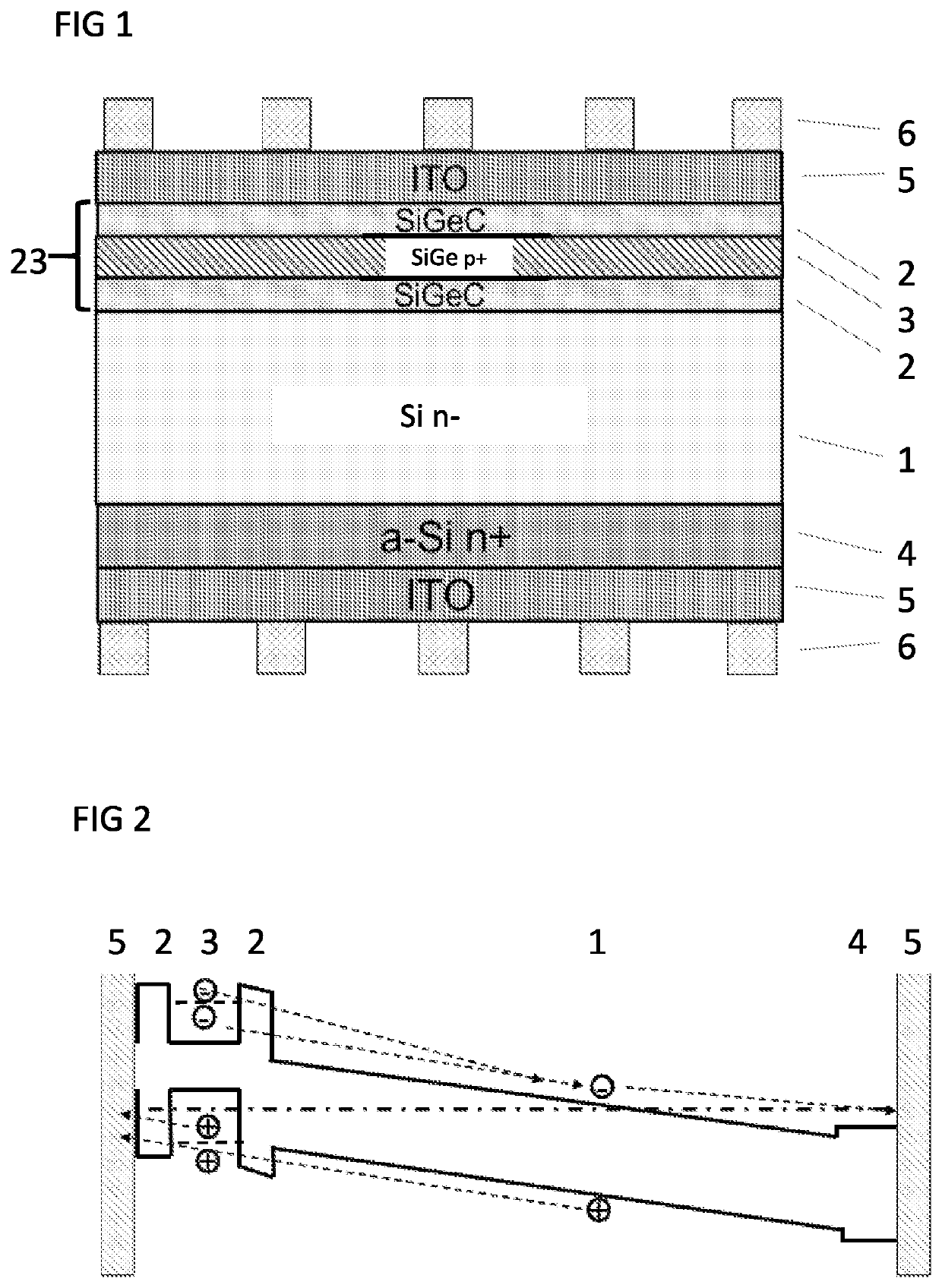
[0036]FIGS. 1 and 2 show an example of a semiconductor component 10 in the form of a single-stage solar cell with a highly doped emitter made of a SiGe quantum structure. In this case, FIG. 1 describes the layer structure and FIG. 2 describes the electrical band structure.

[0037]Starting from a low-doped 1-2 Ω-cm n-type PV wafer 1, a quantum structure emitter 23 consisting of a triple layer 2, 3, 2 is located on a top side. The two outer layers 2 are each a layer of SiC, GeC or SiGeC. These layers 2 are distinguished above all in that they have a significantly higher band gap than Si. In the case of Si, the band gap is approximately 1.1 eV, whereas the band gap of the layers 2, as shown in FIG. 2, is typically between 2 eV and 3.4 eV.

[0038]It is also possible for these layers 2 to be formed, for example, of SiO2 or Al2O3 in order to form so-called tunnel barriers. This function also determines the thickness of the layers 2, which is particularly preferably less than 10 nm, in order t...


PUM

PropertyMeasurementUnit
band gapaaaaaaaaaa
band gapaaaaaaaaaa
thicknessaaaaaaaaaa

Abstract

A semiconductor device having a highly doped quantum structure emitter is disclosed. In an embodiment, the semiconductor device includes a quantum structure emitter. The quantum structure emitter includes of a first layer made of an undoped semiconductor material with a large band gap, a second, middle, highly doped layer made of a semiconductor material with a low band gap and a third, undoped layer made of a semiconductor material with a large band gap.

Description

[0001]This patent application is a national phase filing under section 371 of PCT / EP2018 / 082222, filed Nov. 22, 2018, which claims the priority of European patent application 17209638.0, filed Dec. 21, 2017, each of which is incorporated herein by reference in its entirety.TECHNICAL FIELD[0002]A semiconductor component, in particular a solar cell, comprising a highly doped quantum structure emitter is provided.BACKGROUND[0003]Silicon solar cells are produced and marketed commercially on a grand scale since the beginning of this chiliad. There are currently the following important technologies with the following performance efficiencies:[0004]World records: Crystalline III-V, 44.7%, thin film a-Si / c-Si, 20.8%, thin Film CIGS, 20.5%, thin film CdTe, 21.0% and crystalline silicone, 25.6%.[0005]Production:[0006]Crystalline III-V, 25%, thin film a-Si, 19% and thin Film CIGS, 10% to 13%.[0007]Solar cells based on crystalline silicon: Standard Silicone, 18% to 19%, PERC, 20% to 21%, HJT, 2...

Claims


Application Information

Patent Timeline
Patent Type & Authority Applications(United States)
IPC IPC(8): H01L31/0725H01L31/0352
CPCH01L31/035209H01L31/0725H01L31/035254Y02E10/50
Inventor SCHUEPPEN, ANDREAS PAULSTOWASSER, RAINER
Owner AE 111 AUTARKE ENERGIE GMBH
Why Eureka
Try Eureka