
Array substrate, display panel, and display device

a display panel and substrate technology, applied in non-linear optics, instruments, optics, etc., can solve the problems of character discoloration trail, inconsistent response time of subpixel units of different colors, and significant degrading user experien

Active Publication Date: 2019-08-01
XIAMEN TIANMA MICRO ELECTRONICS
View PDF0 Cites 0 Cited by
  • Summary
  • Abstract
  • Description
  • Claims
  • Application Information

AI Technical Summary

Benefits of technology

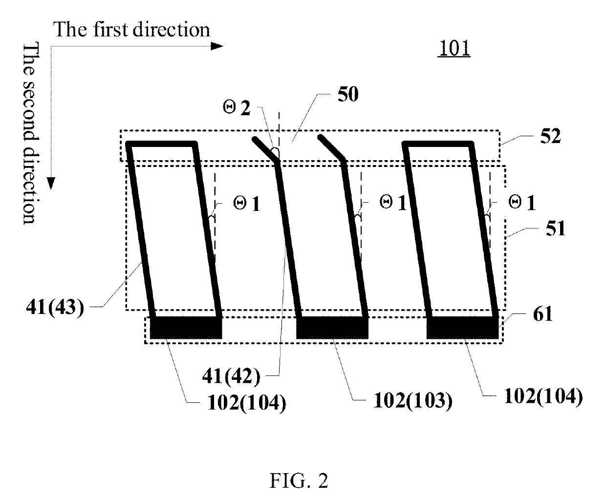
The patent text describes a solution for a display panel to improve response time and prevent the decrease of transmittance. The solution involves adding an adjustment-subpixel region with an opening at the end points, away from the first straight portions, between adjacent second portions of second electrodes. The angle between a straight portion and the second direction is set to be greater than the angle between the first straight portion and the second direction. This design helps to speed up the pixel response time, reduce the discrepancy in response time, improve motion blur and discoloration, and overcome other technical problems in existing technologies.

Problems solved by technology

This leads to an inconsistent response time for subpixel units of different colors.
Due to the inconsistent response time for different colors, a character discoloration trail is prone to occur.
And the larger the discrepancy in the response time of the subpixel units of different colors is, the more evident the discoloration trail will be, thereby significantly degrading user experience.

Method used


Image

  • Array substrate, display panel, and display device
  • Array substrate, display panel, and display device
  • Array substrate, display panel, and display device

Examples


Embodiment Construction

[0035]Certain terms are used throughout the description and claims to refer to particular components. Those skilled in the art should understand that hardware manufactures may use different terms to refer to the same component. The description and the claims do not use the difference in names as a means of distinguishing the components, but use the difference in the functions of the components as the criteria for differentiation. As used throughout the specification and claims, “comprising” is an open language and should the be interpreted as “including but not limited to”. “Approximately” means that within an acceptable error range, those skilled in the art can solve the technical problem within the certain error range and basically can achieve the technical effect. Furthermore, the term “couple” hereby may include any direct and indirect electrical coupling manners. Hence, if a first device is described as being coupled to a second device, it represents that the first device can h...


PUM


Abstract

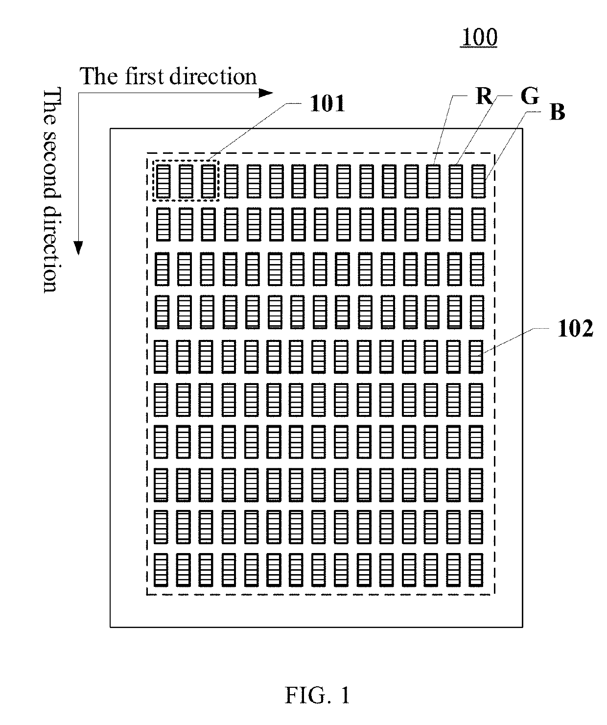
An array substrate, a display panel, and a display device are provided. The array substrate comprises a plurality of pixel regions in an array along intersected first and second directions. The pixel region includes at least three subpixel regions. At least one subpixel region serves as an adjustment-subpixel region. The subpixel region has a first electrode including at least two parallel first straight portions. Second straight portions and first connecting portions are connected to first and second ends of the first straight portions, respectively. The first electrode corresponding to the adjustment-subpixel region serves as an adjustment electrode. An opening is configured at an end between the at least two adjacent second straight portions corresponding to the adjustment electrode. An angle between extending direction of the first straight portion and the second direction is less than an angle between extending direction of the second straight portion and the second direction.

Description

CROSS-REFERENCES TO RELATED APPLICATIONS[0001]This application claims priority of Chinese Patent Application No. 201810098638.1, tiled on Jan. 31, 2018, the entire contents of which are hereby incorporated by reference.FIELD OF THE INVENTION[0002]The present disclosure generally relates to the field of display technology and, more particularly, relates to an array substrate, a display panel, and a display device.BACKGROUND[0003]Liquid crystal display (LCD) equipment has been widely applied in various fields due to its advantages of small size, light weight, and low radiation, etc. LCD panel is the most important element of an LCD equipment The working principle of LCD is: through the adjustment of a voltage applied to a liquid-crystal layer, changing a rotation degree of liquid-crystal molecules, thereby controlling a rotation direction of the polarized light and polarization states, and achieving the alteration of display states of LCD.[0004]Moreover, touch screen technology has gr...

Claims


Application Information

Patent Timeline
IPC IPC(8): G02F1/1343G02F1/1368
CPCG02F1/134336G02F1/1368G02F2201/123G02F2201/122G02F2001/13685G02F1/134363G02F2001/133397G02F1/134309G02F1/133397G02F1/133707G02F1/13685
Inventor LIANG, YUJIAOFANG, LITINGLING, ANKAIYU, YANPINGSHEN, BOPING
Owner XIAMEN TIANMA MICRO ELECTRONICS
Learn More