LCD Monitor

A liquid crystal display, pixel electrode technology, applied in the direction of instruments, nonlinear optics, optics, etc., can solve the problems of reducing the aperture ratio of liquid crystal display, etchant damage, common voltage transmission line and gate line short circuit, etc.

Active Publication Date: 2017-11-21
SAMSUNG DISPLAY CO LTD
View PDF6 Cites 0 Cited by
  • Summary
  • Abstract
  • Description
  • Claims
  • Application Information

AI Technical Summary

Problems solved by technology

[0004] However, during the fabrication of such devices (with pixel and common electrodes on the same substrate), new problems gradually arise
The first such problem is that the optical transmittance may be reduced by the haze effect caused by chemical reduction reactions that may occur between these two electrodes
Furthermore, if a pixel electrode is formed to directly contact the drain electrode of a corresponding thin film transistor (TFT) or another such switching element, the drain electrode can be damaged by the etchant used to pattern the pixel electrode
In addition, in order to connect the common electrode to the common voltage line for transmitting the common electrode voltage thereto, it may be necessary to form a contact hole, resulting in a decrease in the aperture ratio of the liquid crystal display.
In addition, the common voltage transmission line and the gate line may become short-circuited to each other, for example, due to static electricity generated at the time of forming the drain contact hole
[0005] Also, as liquid crystal displays generally increase in size (due to market demand), the number of data lines provided on one substrate tends to increase, and the cost of data drivers for driving these data lines also tends to increase, thereby increasing the liquid crystal display. The overall manufacturing cost of the display

Method used


Image

  • LCD Monitor
  • LCD Monitor
  • LCD Monitor

Examples


Embodiment Construction

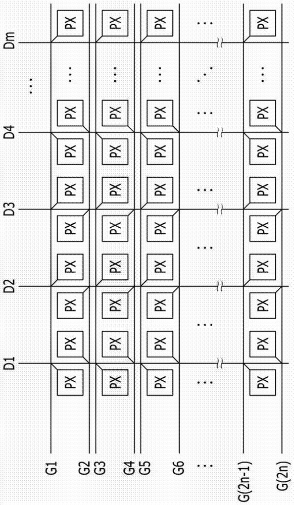
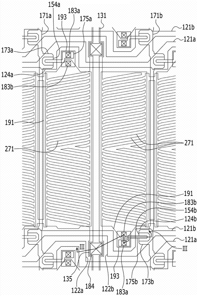
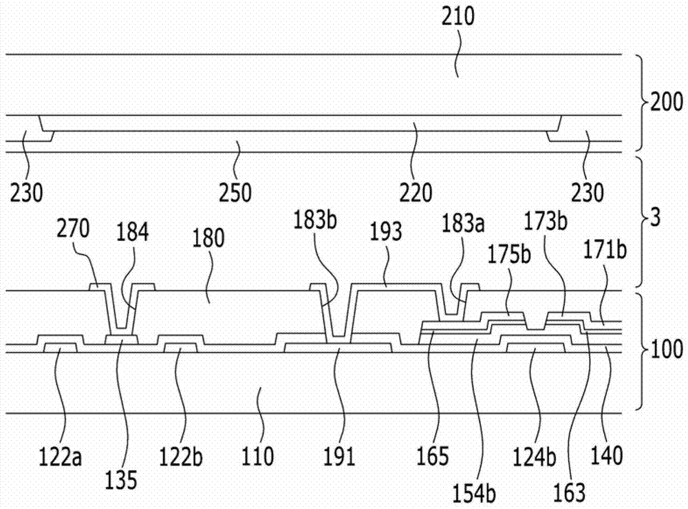
[0026] In the following, the present invention will be described more fully with reference to the accompanying drawings, in which exemplary embodiments according to the teachings of the invention are shown. As those skilled in the art would realize, from the present disclosure, the described embodiments may be modified in various different ways, all without departing from the spirit or scope of the teachings of the present invention.

[0027] In the drawings, the thickness of layers, films, panels, regions, etc., are generally exaggerated for clarity. Like reference numerals refer to like elements throughout the specification. It will be understood that when an element such as a layer, film, region, or substrate is referred to as being "on" another element, it can be directly on the other element or intervening elements may also be present. In contrast, when an element is referred to as being "directly on" another element, there are no intervening elements present.

[0028] ...


PUM


Abstract

The invention discloses a liquid crystal display. The liquid crystal display uses a layout that reduces the number of data lines relative to the number of pixel columns by providing one data line for every two pixel columns. The display is configured to prevent the passivation layer from becoming opaque due to the haze effect of the fabrication by forming the pixel electrodes under the gate insulating layer. The display is configured to prevent damage to the drain electrodes due to the etchant used to pattern the pixel electrodes. In addition, the display is configured to prevent a short circuit between the common voltage line and the gate line without substantially lowering the opening by providing the common voltage contact hole between the vertically extending portions of the two gate lines extending generally horizontally The common voltage contact hole is used to electrically connect the common voltage line with the common electrode.

Description

technical field [0001] The invention relates to a liquid crystal display. Background technique [0002] Liquid crystal displays (LCDs) are one of the most common types of flat panel displays in use today. An LCD is a display device in which liquid crystal molecules of a liquid crystal layer are rearranged by applying an electric field across the liquid crystal layer so that the LC molecules are reoriented and their optical properties are used to control the amount of transmitted light. An electric field across the liquid crystal layer is typically created by applying a voltage between a so-called pixel electrode and an opposing common electrode. In one type of LCD, pixel electrodes and opposing common electrodes are respectively disposed on separate substrates. In the second type of LCD, a pixel electrode and an opposite common electrode are integrally disposed on the same substrate. [0003] Liquid crystal type displays have advantages such as being easy to make thin, bu...

Claims


Application Information

Patent Timeline
Patent Type & Authority Patents(China)
IPC IPC(8): G02F1/1362G02F1/1368G02F1/1343
CPCG02F1/134363G02F1/136227G02F1/136286G02F1/1343
Inventor 朴京淳金一坤崔仙暎金性勋
Owner SAMSUNG DISPLAY CO LTD
Why Eureka
Try Eureka