Low contact resistance nanowire fets

a nanowire and low contact resistance technology, applied in the field of fieldeffect transistors, can solve the problems of reducing the cross-sectional area for the difficult formation of s/d regions, affecting device efficiency and speed, etc., and achieve the effect of low contact resistan

Active Publication Date: 2019-09-12
IBM CORP
View PDF5 Cites 10 Cited by
  • Summary
  • Abstract
  • Description
  • Claims
  • Application Information

AI Technical Summary

Benefits of technology

[0003]In accordance with an embodiment of the present invention, a method for forming a low contact resistance nanowire transistor. The method includes forming a stack of nanowires having alternating nanowire layers including first nanowires and second nanowires. Further included is a step for recessing each of the first nanowires such that each of the second nanowires extend beyond the first nanowires. Source and drain regions are grown from surfaces of the second nanowires beyond a width defined by outer surfaces of gate spacers such that the second nanowires extend into the source and drain regions outside of the width defined by outer surfaces of gate spacers. A gate is formed between the gate spacers including replacing the recessed first nanowires with a gate conductor such that the second nanowire extends through the gate conductor.

Problems solved by technology

However, shrinking source and drain (S / D) regions of the FETs that contact the semiconductor of the CMOS for the movement of current across the device from source to drain can result in a reduced cross-sectional area for the formation of the S / D regions.
This process can make the formation of the S / D regions difficult and can affect the efficiency and speed of the device.

Method used


Image

  • Low contact resistance nanowire fets
  • Low contact resistance nanowire fets
  • Low contact resistance nanowire fets

Examples


Embodiment Construction

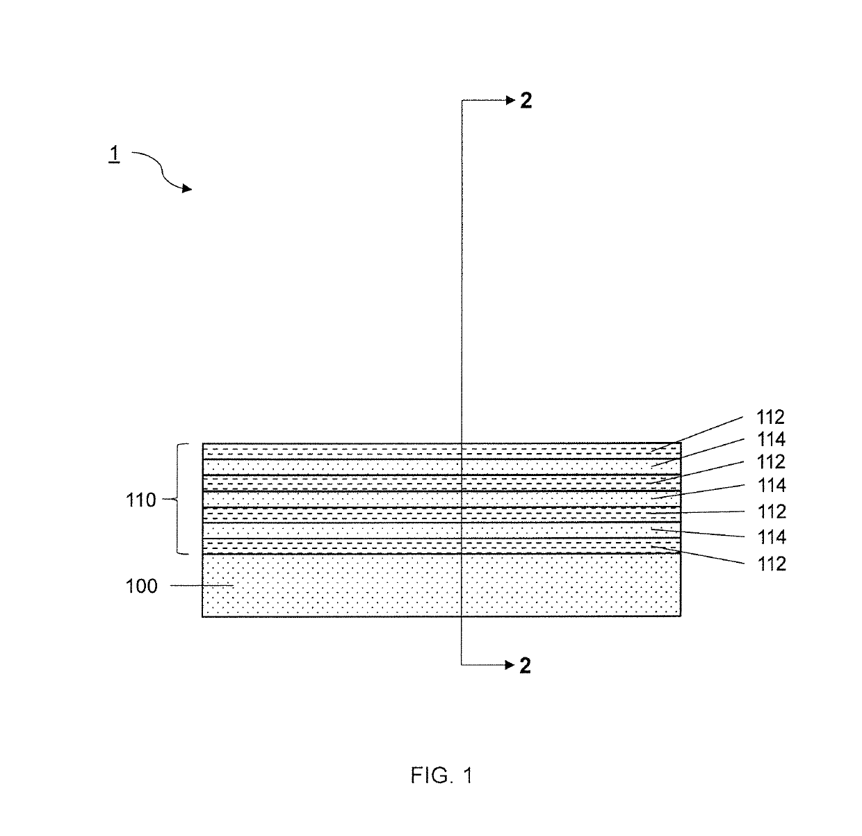
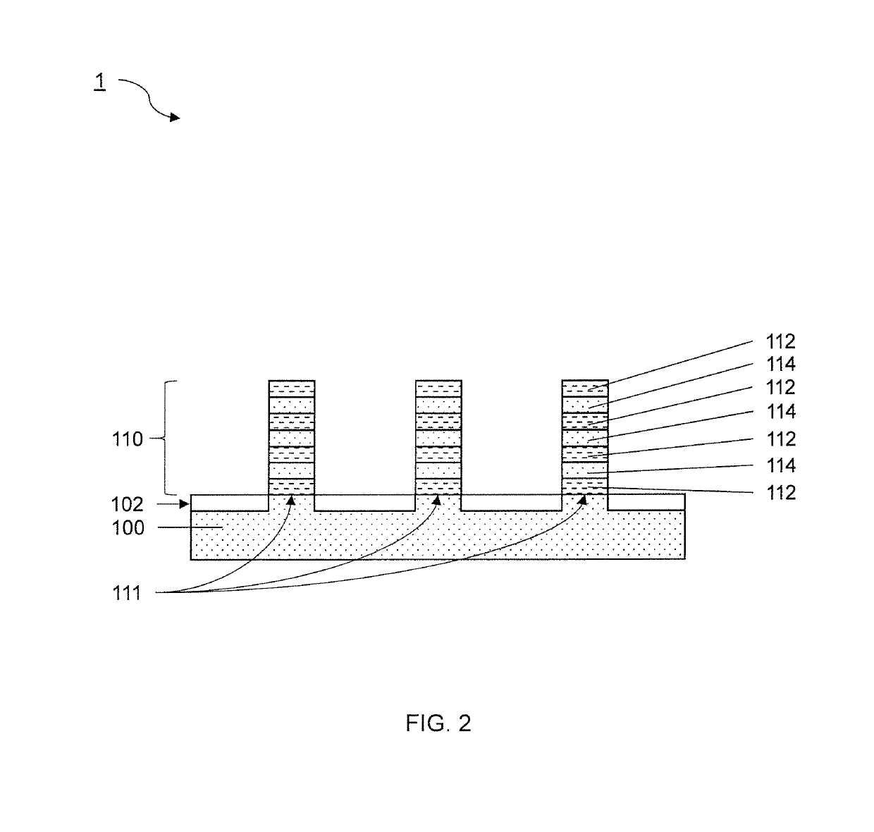
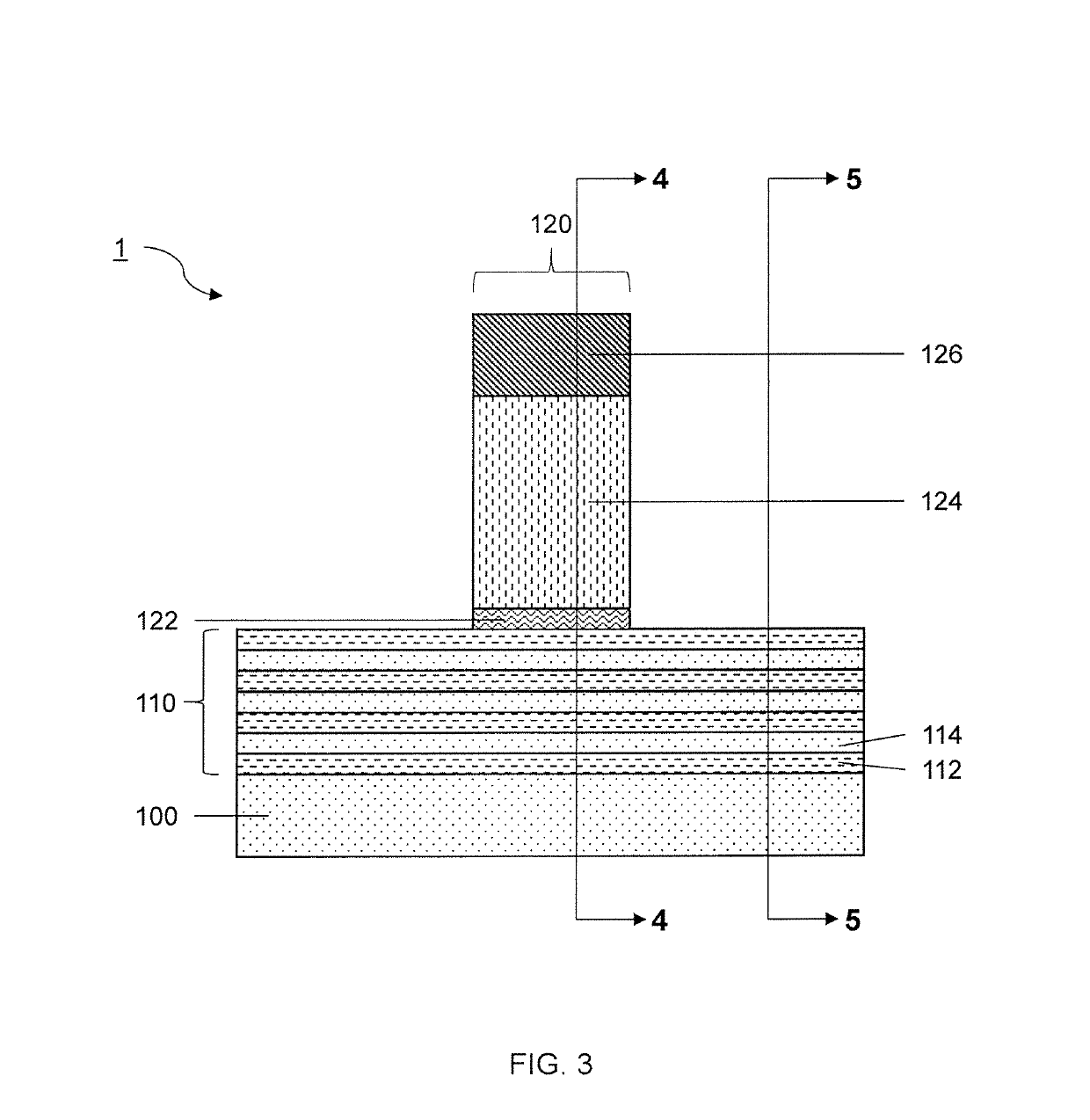
[0038]Shrinking the size of semiconductor devices is useful for decreasing device real-estate, as well as improving the efficiency and speed of the devices. Such devices can include field-effect transistors (FETs). By incorporating nanowires into the semiconductor devices, including FETs, the electrical properties of the devices can be improved, enabling a decrease in size of the devices. However, decreasing the size of the devices, S / D regions will become harder to form due to decreased surface area of the nanowires.

[0039]To facilitate further decrease in semiconductor device size, nanowire FETs with unchopped nanowires are contemplated. These nanowire FETs are formed from nanowire semiconductors in, e.g., fin configurations. A gate can be formed over the fins of the nanowire FETs, with sacrificial nanowires being recessed. However, the semiconductor nanowires are not recessed. Rather, a fill material is employed to fill a device region such that, upon annealing the fill material, ...


PUM


Abstract

Systems and methods for forming a low contact resistance nanowire transistor are described. The transistor includes a gate formed over a substrate including a gate conductor. Gate spacers are formed on sides of the gate. At least one semiconductor nanowire is formed through the gate such that the at least one semiconductor nanowire extends through the gate conductor and the gate spacers and into source and drain regions grown from surfaces of the at least one semiconductor nanowire adjacent to sides of the gate to increase the surface area of the source drain region contacting the semiconductor nanowire.

Description

BACKGROUNDTechnical Field[0001]The present invention generally relates to the formation of field-effect transistors (FETs), and more particularly to the formation of low contact resistance nanowire FETs.Description of the Related Art[0002]Complimentary metal-oxide semiconductors (CMOS) provide benefits to the speed and efficiency of field-effect transistors (FETs), and other devices. However, shrinking source and drain (S / D) regions of the FETs that contact the semiconductor of the CMOS for the movement of current across the device from source to drain can result in a reduced cross-sectional area for the formation of the S / D regions. This process can make the formation of the S / D regions difficult and can affect the efficiency and speed of the device.SUMMARY[0003]In accordance with an embodiment of the present invention, a method for forming a low contact resistance nanowire transistor. The method includes forming a stack of nanowires having alternating nanowire layers including fir...

Claims


Application Information

Patent Timeline
Patent Type & Authority Applications(United States)
IPC IPC(8): H01L29/06H01L29/08H01L21/02H01L29/66H01L21/3065H01L29/423H01L29/78H01L29/786
CPCH01L29/6656H01L29/66742H01L29/0673H01L29/0847H01L29/66545H01L29/42392H01L21/3065H01L29/78651H01L21/02112H01L21/02532H01L21/31053H01L29/66795H01L29/66553H01L29/785H01L29/78696H01L29/66439
Inventor XU, PENGLI, JUNTAOLEE, CHOONGHYUNCHENG, KANGGUO
Owner IBM CORP
Why Eureka
Try Eureka