Targeted Recall of Semiconductor Devices Based on Manufacturing Data

a technology of manufacturing data and semiconductor devices, applied in semiconductor/solid-state device testing/measurement, semiconductor/solid-state device details, instruments, etc., can solve problems such as ineffective blanket recalls, inefficient or ineffective at preventing the same or similar types of failures, and inability to accurately predict device failures to provide targeted recalls

Active Publication Date: 2019-09-26
KLA TENCOR TECH CORP
View PDF5 Cites 16 Cited by
  • Summary
  • Abstract
  • Description
  • Claims
  • Application Information

AI Technical Summary

Benefits of technology

[0005]A system for providing a targeted recall is disclosed in accordance with one or more illustrative embodiments of the present disclosure. In one illustrative embodiment, the system includes a metrology sub-system for performing in-line measurements on semiconductor dies after one or more fabrication steps to generate in-line measurement profiles. In another illustrative embodiment, the metrology sub-system performs one or more measurements of the semiconductor dies after one or more packaging steps to generate package characterization profiles. In another illustrative embodiment, the system includes a failure analysis sub-system for determining at least a portion of a manufacturing fingerprint of a failed die. In another illustrative embodimen...

Problems solved by technology

Product recalls due to failures of semiconductor devices are typically costly and disruptive for both businesses and consumers.
However, such blanket recalls may be inefficient or ineffective at preventing the same or similar types of failures in the future.
Failure of a...

Method used


Image

  • Targeted Recall of Semiconductor Devices Based on Manufacturing Data
  • Targeted Recall of Semiconductor Devices Based on Manufacturing Data
  • Targeted Recall of Semiconductor Devices Based on Manufacturing Data

Examples


Embodiment Construction

[0018]Reference will now be made in detail to the subject matter disclosed, which is illustrated in the accompanying drawings. The present disclosure has been particularly shown and described with respect to certain embodiments and specific features thereof. The embodiments set forth herein are taken to be illustrative rather than limiting. It should be readily apparent to those of ordinary skill in the art that various changes and modifications in form and detail may be made without departing from the spirit and scope of the disclosure.

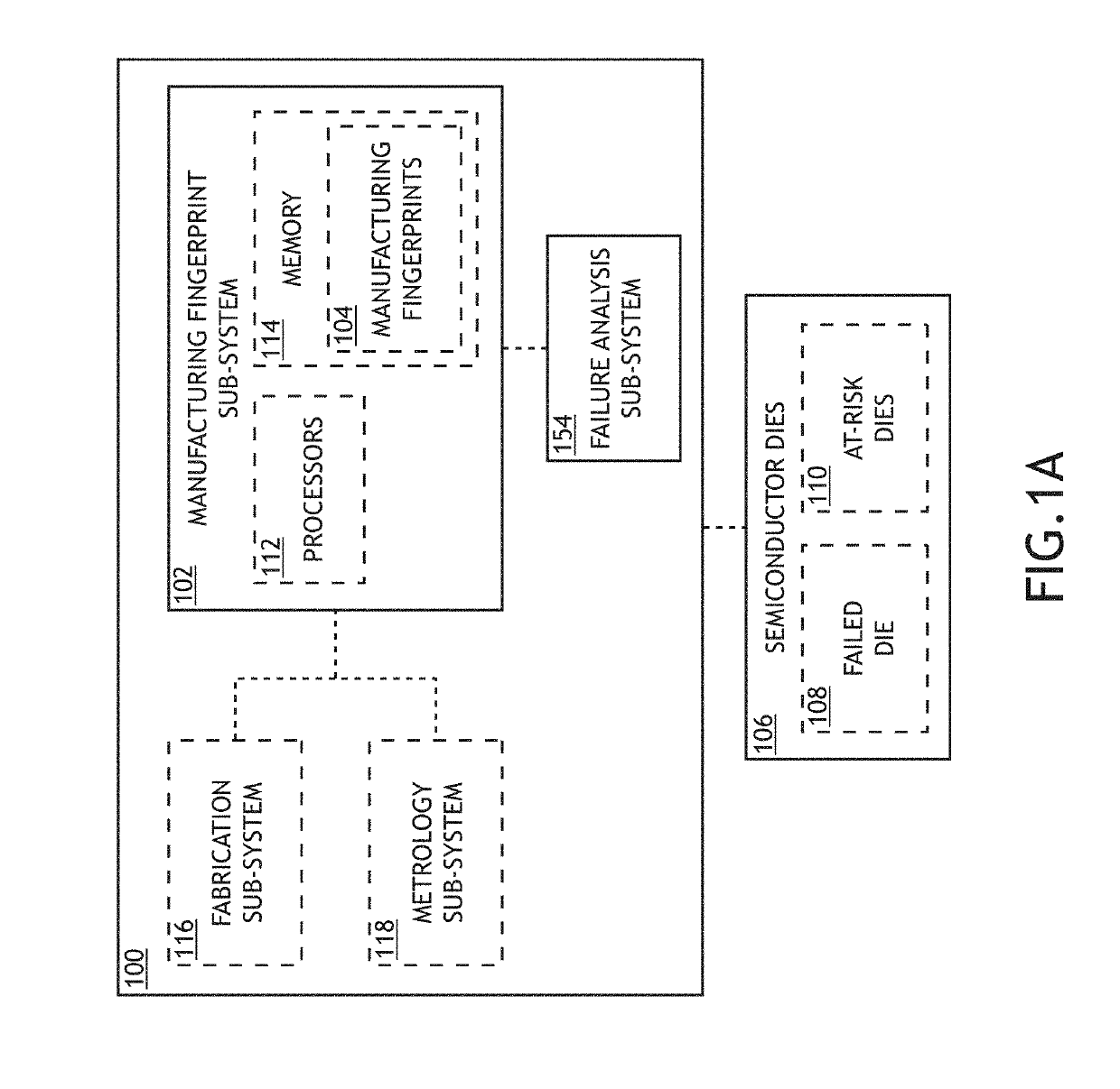
[0019]Embodiments of the present disclosure are directed to systems and methods for providing targeted recalls of semiconductor devices based on holistic manufacturing data.

[0020]In some embodiments, manufacturing fingerprints (e.g., fingerprints) are developed to consolidate and / or track data relevant to the manufacturing history of semiconductor devices such as, but not limited to, fabrication profiles, in-line measurement profiles, package test pr...


PUM


Abstract

A system for providing a targeted recall includes a metrology sub-system for performing in-line measurements on semiconductor dies after one or more fabrication steps to generate in-line measurement profiles, a failure analysis sub-system for determining a manufacturing fingerprint of a failed die, and a controller. The metrology sub-system may further perform one or more measurements of the semiconductor dies after one or more packaging steps to generate package characterization profiles. The controller may generate manufacturing fingerprints for the semiconductor dies based on the in-line measurement profiles and the package characterization profiles, which are referenced to unique electronic chip identifiers. The controller may further identify at-risk dies by comparing the manufacturing fingerprints of the semiconductor dies with the manufacturing fingerprint of the failed die and direct a targeted recall for the one or more at-risk dies.

Description

CROSS-REFERENCE TO RELATED APPLICATION[0001]The present application claims the benefit under 35 U.S.C. § 119(e) of U.S. Provisional Application Ser. No. 62 / 645,406, filed Mar. 20, 2018, entitled METHOD TO ENABLE TARGETED RECALL LOF AT RISK SEMICONDUCTOR DEVICES USING HOLISTIC MANUFACTURING DATA AND MACHINE LEARNING, naming Robert J. Rathert and David W. Price as inventors, which is incorporated herein by reference in the entirety.TECHNICAL FIELD[0002]The present disclosure is related to recalls of semiconductor devices and, more particularly, to target recalls of semiconductor devices based on manufacturing data.BACKGROUND[0003]Product recalls due to failures of semiconductor devices are typically costly and disruptive for both businesses and consumers. It is thus desirable to limit recalls to semiconductor devices that are expected to fail in order to mitigate the associated cost and disruption. Typical product recalls are based on gross attributes associated with a failed device s...

Claims


Application Information

Patent Timeline
IPC IPC(8): H01L21/66G01R31/28G06Q30/00
CPCG01R31/2831G06Q30/014H01L22/34H01L22/12H01L22/14H01L22/20H01L23/544H01L2223/54433G01R31/2894H01L21/67242H01L22/10H01L22/30
Inventor RATHERT, ROBERT J.PRICE, DAVID W.
Owner KLA TENCOR TECH CORP
Why Eureka
Try Eureka