Apparatus and method for inspecting substantially transparent electronic devices
- Summary
- Abstract
- Description
- Claims
- Application Information
AI Technical Summary
Benefits of technology
Problems solved by technology
Method used
Image

Examples
Embodiment Construction
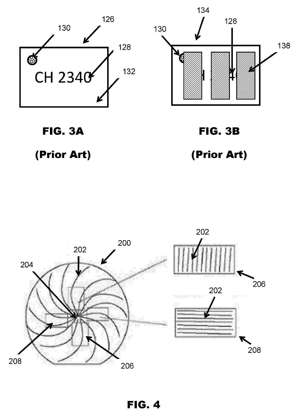
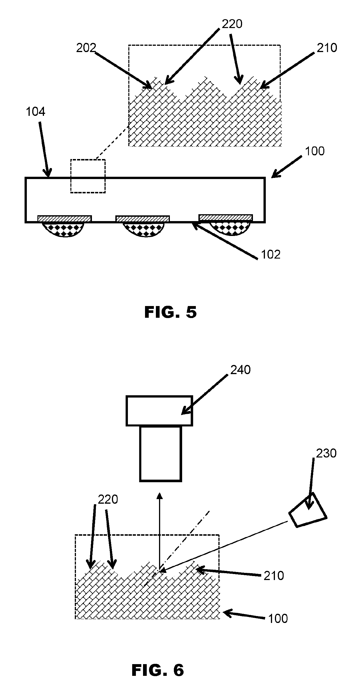
[0027]A back-side of a wafer 200 is usually grinded prior to singulation, in order to reduce a thickness of the wafer 200 after fabrication. The back-side grinding process typically produces curved grinding marks 202 on the surface of the grinded surface, where the curved grinding marks 202 extend radially from approximately a centre 204 of the wafer 200 towards a circumference of the wafer 200, as shown in FIG. 4. Although the grinding marks 202 are generally curved, it has been observed that the grinding marks 202 in relatively small localized portions 206, 208 of the wafer 200 appear to be substantially parallel, as illustrated in FIG. 4. In each localized portion 206, 208, the grinding marks 202 are substantially parallel, and typically deviate from one another by less than 10°. Hence, for a wafer 200 which is 8 inches in diameter, the grinding marks 202 in the localized portions 206, 208 with surface areas of about 2 mm2 would appear to be substantially parallel. As such, singu...
PUM
 Abstract
Description
Claims
Application Information
 - R&D Engineer
- R&D Manager
- IP Professional
- Industry Leading Data Capabilities
- Powerful AI technology
- Patent DNA Extraction
Browse by: Latest US Patents, China's latest patents, Technical Efficacy Thesaurus, Application Domain, Technology Topic.
© 2024 PatSnap. All rights reserved.Legal|Privacy policy|Modern Slavery Act Transparency Statement|Sitemap