Structure with micro device
a micro-device and structure technology, applied in the direction of micro-devices, basic electric elements, electrical equipment, etc., can solve the problems of easy affecting quality of micro-leds and yield rate of delivery, and achieve the effect of improving the yield rate of delivery and transfer of micro-devices
- Summary
- Abstract
- Description
- Claims
- Application Information
AI Technical Summary
Benefits of technology
Problems solved by technology
Method used
Image
Examples
first embodiment
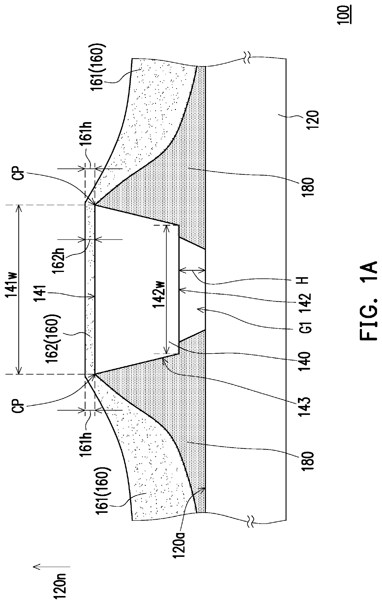
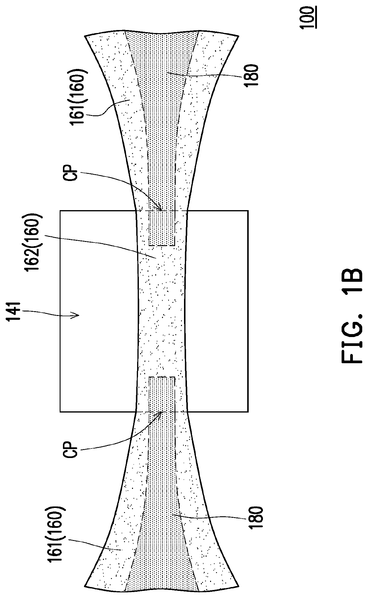
[0046]FIG. 1A is a schematic cross-sectional view of a structure with micro device according to the invention. FIG. 1B is a schematic top view of the structure with micro device in FIG. 1A. Referring to FIG. 1A, a structure with micro device 100 in the embodiment includes a substrate 120, at least one micro device 140, and at least one holding structure 160 and at least one buffering structure 180. The micro device 140 is disposed on the substrate 120 and has a top surface 141 relatively far away from the substrate 120, a bottom surface 142 opposite to the top surface 141 and a peripheral surface 143 connecting the top surface 141 and the bottom surface 142. The holding structure 160 is disposed on the substrate 120. From the cross-sectional view, the thickness of the holding structure 160 in a normal direction 120n of the substrate 120 is gradually increased from a boundary CP between the top surface 141 and the peripheral surface 143 of the micro device 140 to the substrate 120. T...
fifth embodiment
[0060]FIG. 6A is a partial schematic cross-sectional view of a structure with micro device according to another embodiment of the invention. FIG. 6B is a schematic top view of the structure with micro device in FIG. 6A. FIG. 6C is a schematic three-dimensional view of the structure with micro device in FIG. 6A. Referring to FIG. 6A, a structure with micro device 600a of the embodiment is similar to the structure of the micro device 400 of the fifth embodiment, and the difference between the two is that the thickness of the holding structure 660a is not fixed from the boundary between the top surface 641 and the peripheral surface 643a of the micro device 640a to the substrate 620. The micro device 640a is directly connected to the substrate 620 through the holding structure 660a. Specifically, the horizontal distance H1, H2 between the holding structure 660a and the substrate 620 in a direction parallel to the substrate 620 is gradually increased from the boundary between the top su...
PUM
 Abstract
Description
Claims
Application Information


