Switching device

a technology of switching device and switch, which is applied in the direction of semiconductor device, semiconductor/solid-state device details, electrical apparatus, etc., can solve the problems of reducing increasing the insertion loss of switches, so as to suppress the increase of insertion loss and reduce the electrical power of signals. , the effect of increasing the insertion loss

Active Publication Date: 2019-12-12
MURATA MFG CO LTD
View PDF0 Cites 0 Cited by
  • Summary
  • Abstract
  • Description
  • Claims
  • Application Information

AI Technical Summary

Benefits of technology

[0006]Here, if the number of input terminals and output terminals is increased, the wires constituting the channels may intersect in multiple metal layers laminated on or above a semiconductor substrate. In the intersection area of the wires, there is a problem that the electric power of signals may be decreased by a parasitic capacitance occurring between the metal layers and the insertion loss in the switch may increase.
[0007]In the light of the above-described circumstances, it is an object of the present disclosure to provide a switching device capable of suppressing an increase in insertion loss.

Problems solved by technology

In the intersection area of the wires, there is a problem that the electric power of signals may be decreased by a parasitic capacitance occurring between the metal layers and the insertion loss in the switch may increase.

Method used


Image

  • Switching device
  • Switching device
  • Switching device

Examples


Embodiment Construction

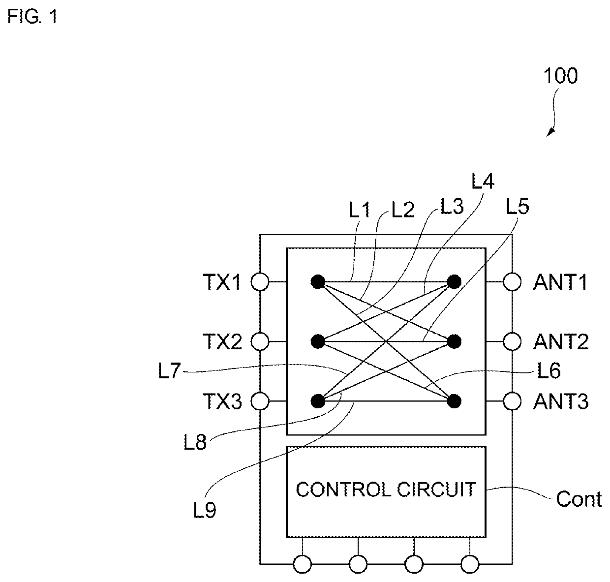
[0016]An embodiment of the present disclosure is described below with reference to the drawings. The same elements have the same reference numerals, and redundant description is omitted.

[0017]FIG. 1 schematically illustrates an example configuration of a switching device according to an embodiment of the present disclosure. A switching device 100 illustrated in FIG. 1 may be incorporated in an apparatus, such as a cellular phone supporting wireless data communications, for example, wireless LAN and Bluetooth (registered mark) communications, and is used for outputting a transmission signal inputted from a transmission circuit to any one of antennas. In the present specification, the switching device 100 is described as being applied to a configuration that transmits transmission signals. The switching device 100 is also applicable to a configuration that supplies reception signals received from antennas to reception circuits.

[0018]The switching device 100 may also be incorporated in...


PUM


Abstract

A switching device includes first to third layers laminated in sequence above a principal surface of a substrate, a plurality of input terminals, a plurality of output terminals, a plurality of switching circuits, and a plurality of channels. Each of the channels electrically connecting one of the plurality of input terminals and one of the plurality of output terminals with one of the plurality of switching circuits interposed therebetween. The plurality of channels include a first channel and a second channel that intersect with each other when the principal surface of the substrate is seen in a plan view. In an intersection area where the first and second channels intersect with each other, the first channel is disposed on the first layer, the second channel is disposed on the third layer, and none of the plurality of channels is disposed on the second layer.

Description

[0001]This is a continuation of International Application No. PCT / JP2018 / 002821 filed on Jan. 30, 2018 which claims priority from Japanese Patent Application No. 2017-036960 filed on Feb. 28, 2017. The contents of these applications are incorporated herein by reference in their entireties.BACKGROUND OF THE DISCLOSUREField of the Disclosure[0002]The present disclosure relates to a switching device.Description of the Related Art[0003]Wireless communication systems, including a wireless local area network (LAN), are required to support transmission and reception of signals in a plurality of kinds of communication standards (multiple modes) and signals in a plurality of kinds of frequency bands (multiple bands). Such an apparatus supporting multiple modes and multiple bands needs to include a plurality of transmission and reception circuits and antennas supporting the modes and the bands and switching circuits that switch a channel between the transmission and reception circuits and the...

Claims


Application Information

Patent Timeline
Patent Type & Authority Applications(United States)
IPC IPC(8): H01L23/528H01L23/50H01L23/66
CPCH01L23/528H01L23/50H01L2223/6605H01L23/66H04B1/0458H01L21/82H01L21/822H01L27/04
Inventor SEKI, KENTA
Owner MURATA MFG CO LTD
Why Eureka
Try Eureka