Inter-board connection structure

Active Publication Date: 2020-01-16
MITSUBISHI ELECTRIC CORP
View PDF0 Cites 2 Cited by
  • Summary
  • Abstract
  • Description
  • Claims
  • Application Information

AI Technical Summary

Benefits of technology

The present invention allows for the downsizing of an impedance matching circuit by eliminating the need for a punched hole in a plate-shaped ground conductor and reducing the size of the third signal line conductor. The capacitive component formed between the first signal pad and the second signal line conductor ensures that capacitance needed for matching of impedance is maintained. This results in a more efficient and compact impedance matching circuit.

Problems solved by technology

However, because a punched hole of the ground conductor causes coupling with a wire located in the inner layer of the dielectric board, there is a case in which such a punched hole cannot be used for an inter-board connection structure.

Method used


Image

  • Inter-board connection structure
  • Inter-board connection structure
  • Inter-board connection structure

Examples


embodiment 1

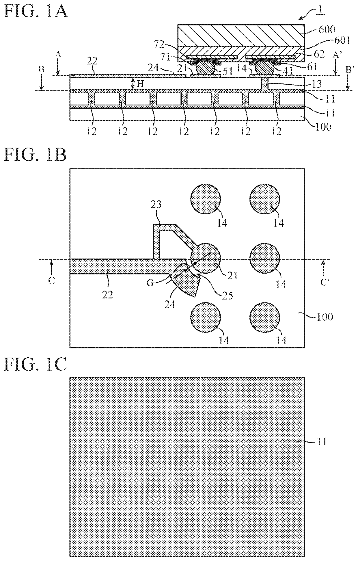
[0027]FIG. 1A is a cross-sectional view showing the configuration of a module 1 provided with an inter-board connection structure according to Embodiment 1 of the present disclosure, and shows a view of the module 1 taken along the C-C′ line of FIG. 1B. FIG. 1B is a cross-sectional view on arrow of the module 1 taken on the plane of the A-A′ line of FIG. 1A. The A-A′ line divides each of the following components: ground pads 14, a signal pad 21, a signal line conductor 22, a signal line conductor 23, and a signal line conductor 24 into two parts in a thickness direction. FIG. 1C is a cross-sectional view on arrow of the module 1 taken on the plane of the B-B′ line of FIG. 1A. The B-B′ line divides a plate-shaped ground conductor 11 into two parts in the thickness direction.

[0028]The module 1 includes a printed circuit board 100 and a semiconductor board 600, and electrode pads between the printed circuit board 100 and the semiconductor board 600 are electrically connected by the int...

embodiment 2

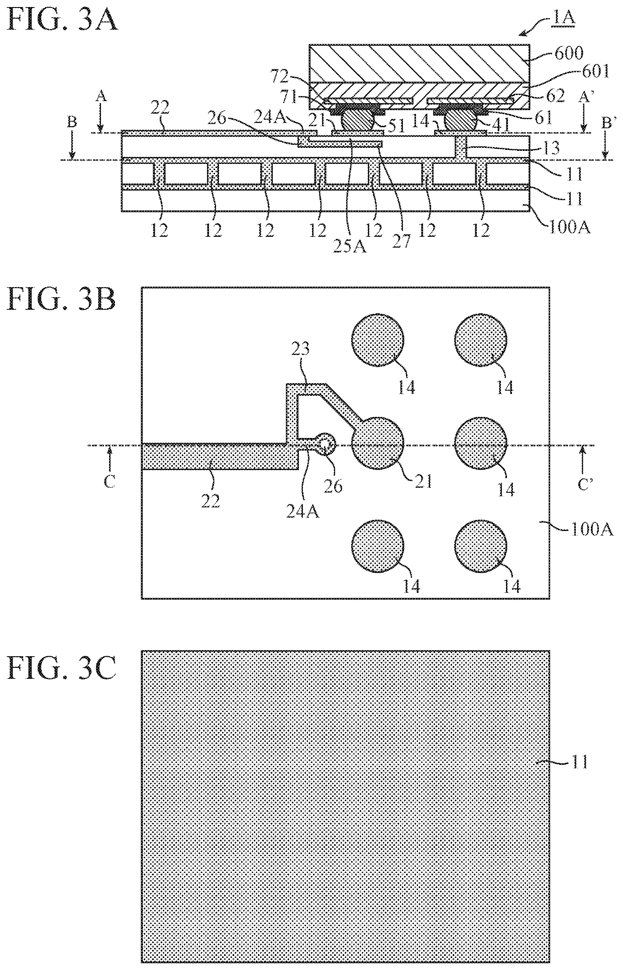
[0058]FIG. 3A is a cross-sectional view showing the configuration of a module 1A including an inter-board connection structure according to Embodiment 2 of the present disclosure, and shows the module 1A taken along the C-C′ line of FIG. 3B. FIG. 3B is a cross-sectional view on arrow of the module 1A taken on the plane of the A-A′ line of FIG. 3A. The A-A′ line divides each of the following components: ground pads 14, a signal pad 21, a signal line conductor 22, a signal line conductor 23, and a signal line conductor 24A into two parts in a thickness direction. FIG. 3C is a cross-sectional view on arrow of the module 1A taken on the plane of the B-B′ line of FIG. 3A. The B-B′ line divides a plate-shaped ground conductor 11 into two parts in the thickness direction.

[0059]In FIGS. 3A, 3B, and 3C, the same components as those shown in FIGS. 1A, 1B, and 1C are denoted by the same reference signs, and an explanation of the components will be omitted hereafter.

[0060]The module 1A includes...

embodiment 3

[0073]FIG. 4A is a cross-sectional view showing the configuration of a module 1B including an inter-board connection structure according to Embodiment 3 of the present disclosure, and shows the module 1B taken along the C-C′ line of FIG. 4B. FIG. 4B is a cross-sectional view on arrow of the module 1B taken on the plane of the A-A′ line of FIG. 4A. The A-A′ line divides each of the following components: ground pads 14, a signal pad 21, a signal line conductor 22, a signal line conductor 23, and a signal line conductor 24B into two parts in a thickness direction. FIG. 4C is a cross-sectional view on arrow of the module 1B taken on the plane of the B-B′ line of FIG. 4A. The B-B′ line divides a plate-shaped ground conductor 11 into two parts in the thickness direction.

[0074]The module 1B includes a printed circuit board 100B and a semiconductor board 600, and electrode pads between the printed circuit board 100B and the semiconductor board 600 are electrically connected by the inter-boa...


PUM


Abstract

Disclosed is an inter-board connection structure including a signal line conductor (22) provided in an outer layer of a printed circuit board (100), a signal line conductor (24) extending in a direction from the signal line conductor (22) to a signal pad (21), and forming a capacitive component between itself and a signal pad (21), and a signal line conductor (23) branching and extending from a connecting portion between the signal line conductor (22) and the signal line conductor (24), and electrically connected to the signal pad (21).

Description

TECHNICAL FIELD[0001]The present disclosure relates to an inter-board connection structure that electrically connects electrode pads between boards by using solder bumps.BACKGROUND ART[0002]In modules of ball grid array (BGA) type, an inter-board connection structure that electrically connects electrode pads between boards by using solder bumps is adopted.[0003]In a conventional inter-board connection structure, in order to reduce a parasitic capacitance component formed between a pad on a dielectric board, and a ground conductor located in an inner layer of the dielectric board, thereby improving the high frequency characteristics, a part of the ground conductor which is directly under the pad is removed to form a punched hole. However, because a punched hole of the ground conductor causes coupling with a wire located in the inner layer of the dielectric board, there is a case in which such a punched hole cannot be used for an inter-board connection structure.[0004]For example, in ...

Claims


Application Information

Patent Timeline
IPC IPC(8): H05K1/02H05K1/11
CPCH05K2201/09281H05K1/025H05K1/113H05K2201/10734H05K2201/09254H05K2201/09727H05K1/181H05K3/3436H05K1/0222H05K1/0298
Inventor YUASA, TAKESHIOSHIMA, TAKESHI
Owner MITSUBISHI ELECTRIC CORP
Why Eureka
Try Eureka