Method for manufacturing semiconductor device

a manufacturing method and semiconductor technology, applied in semiconductor devices, capacitors, electrical devices, etc., can solve the problems of affecting the performance of the semiconductor device, so as to achieve the effect of reducing the capacitor height, stably manufacturing, and simplifying the fabrication process of the semiconductor devi

Inactive Publication Date: 2014-07-29
SK HYNIX INC
View PDF2 Cites 0 Cited by
  • Summary
  • Abstract
  • Description
  • Claims
  • Application Information

AI Technical Summary

Benefits of technology

[0008]An embodiment of the present invention relates to a method for manufacturing a semiconductor device in which a capacitor structure is modified to ensure capacitance of the capacitor, and the height of the capacitor is reduced to prevent defects such as a leaning capacitor or a poor bridge from being generated, such that the fabrication process of semiconductor devices is simplified and therefore the semiconductor devices can be stably manufactured.

Problems solved by technology

However, using the high dielectric material requires time and material investment, for example, the introduction of new equipment or installations, the necessity of verifying the reliability and productivity of a dielectric film, low-temperature processing of a subsequent process, etc.
Specifically, the method for growing the HSG may cause unexpected problems in guaranteeing a Critical Dimension (CD) of at least a predetermined level between lower electrodes, and may cause a bridge between lower electrodes due to infrequent HSG desquamation, so that it is difficult for the aforementioned HSG growing method to be applied to a semiconductor device based on a design rule of 0.14 μm or less.
Provided that the cells share and use such a dielectric material, capacitance (storage capacitance) among all the lower electrodes may be interfered or distorted.
As a result, there arises a bridge between lower electrodes, and it is difficult to guarantee a contact region between the lower electrode contact plug and the lower electrode.

Method used


Image

  • Method for manufacturing semiconductor device
  • Method for manufacturing semiconductor device
  • Method for manufacturing semiconductor device

Examples


Embodiment Construction

[0042]Reference will now be made in detail to embodiments of the present invention, examples of which are illustrated in the accompanying drawings. Wherever possible, the same reference numbers will be used throughout the drawings to refer to the same or like parts. The figures illustrate embodiments of the present invention, but may not be exact representations of the dimensions and shapes that are realized in some embodiments. For example, certain features may be exaggerated or otherwise altered in the figures in order to better illustrate certain inventive concepts.

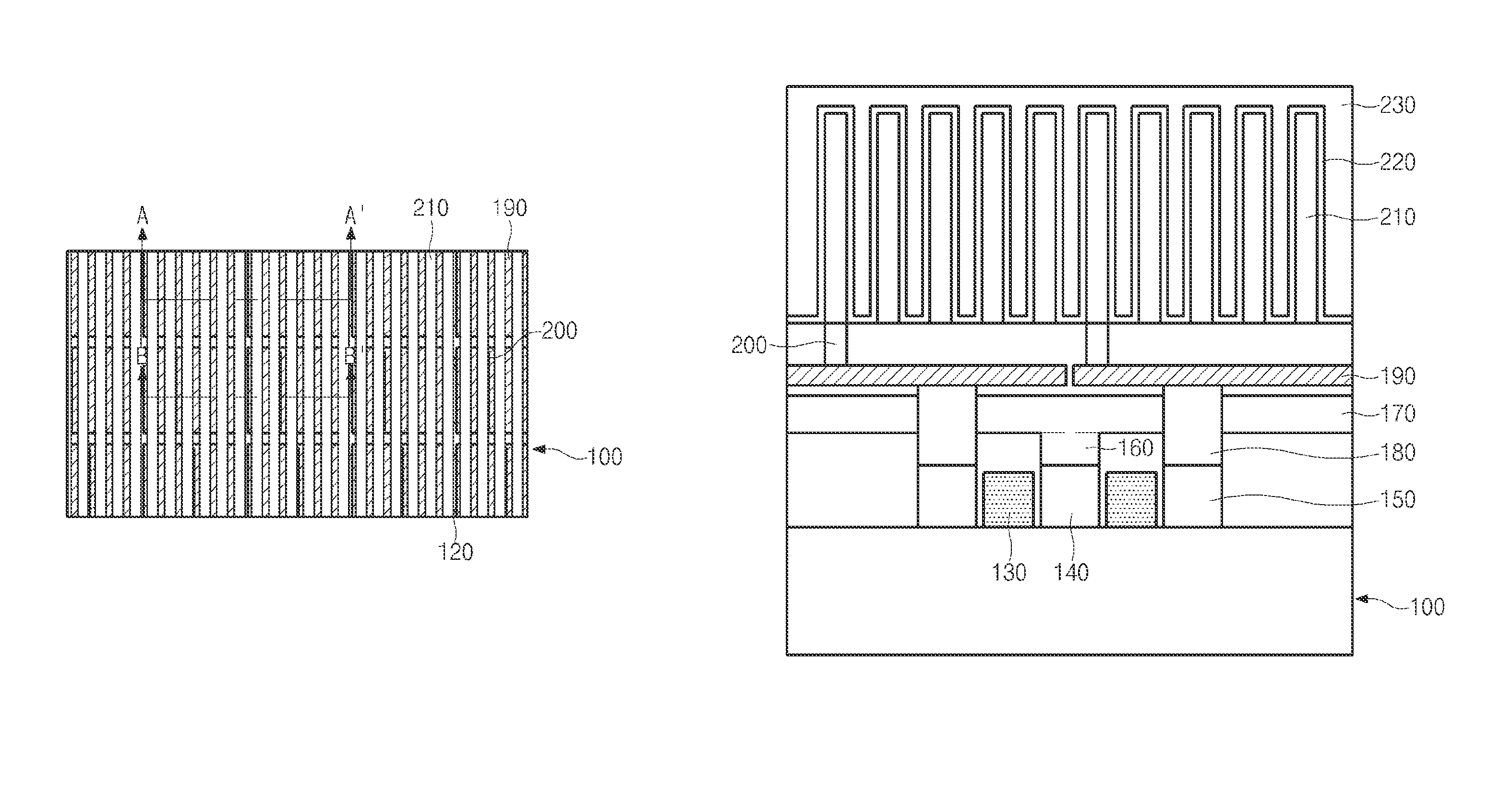
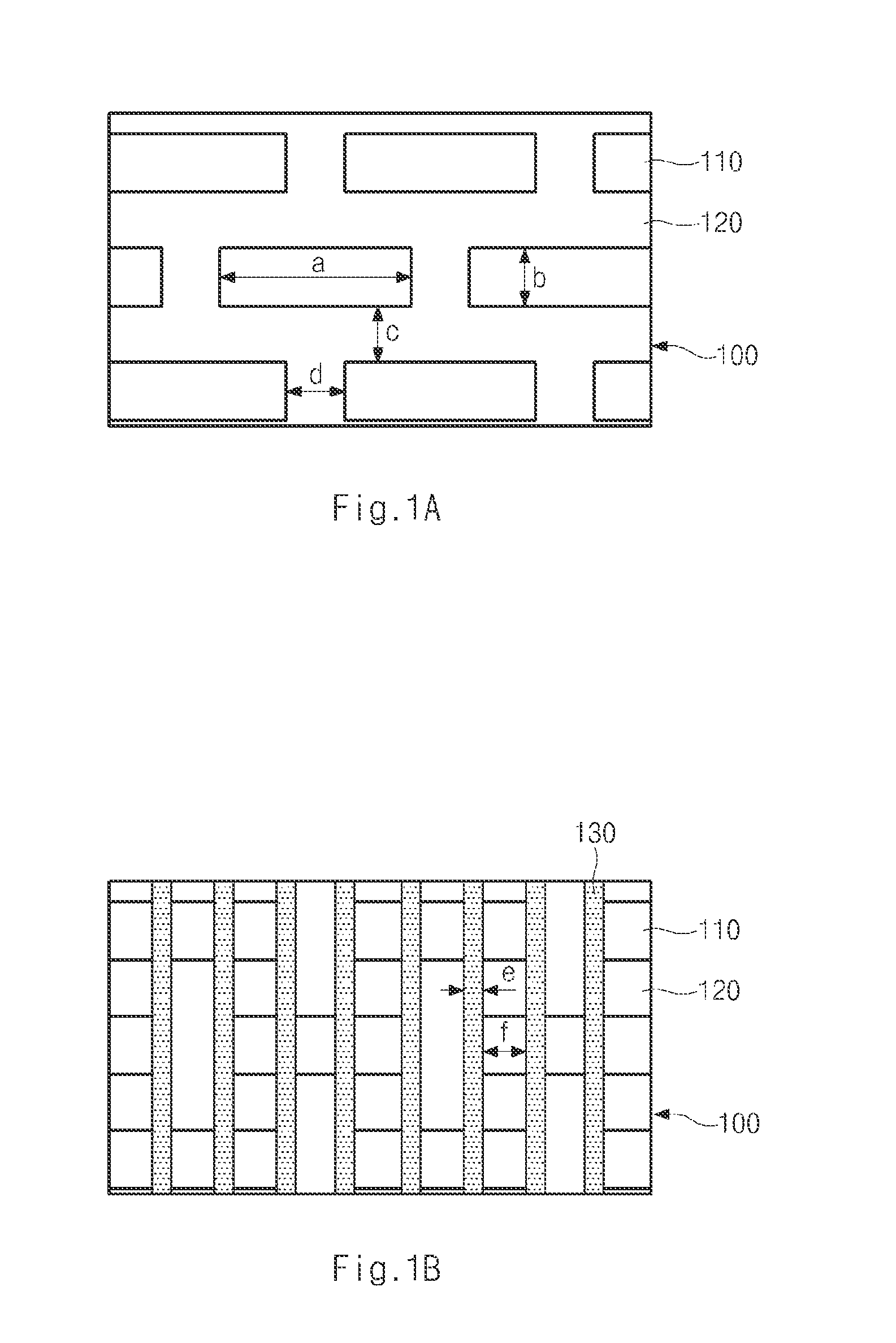
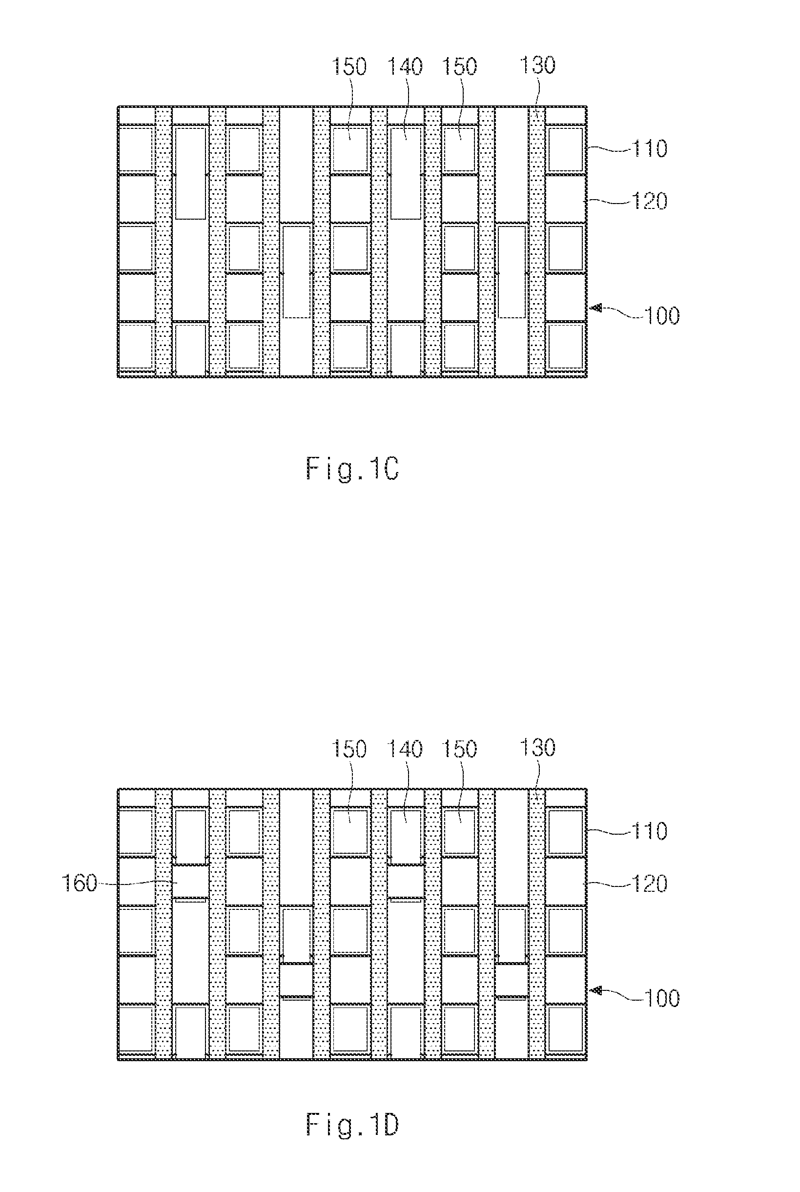
[0043]FIGS. 1A to 1I are layout diagrams illustrating a semiconductor device according to embodiments of the present invention.

[0044]Referring to FIG. 1A, a device isolation film 120 defining an active region 110 is disposed over a semiconductor substrate 100. The active region 110 may be configured in the form of an island, and is formed along a long-axis direction perpendicular to a word line to be formed in a subseq...


PUM


Abstract

A method for manufacturing a semiconductor device is disclosed. In the method for manufacturing the semiconductor device, a capacitor structure is modified to ensure capacitance of the capacitor, and the height of the capacitor is reduced to prevent defects such as a leaning capacitor or a poor bridge from being generated, such that the fabrication process of semiconductor devices is simplified and therefore the semiconductor devices can be stably manufactured.

Description

CROSS-REFERENCE TO RELATED APPLICATION[0001]The priority of Korean patent application No. 10-2011-0051657 filed on 30 May 2011, the disclosure of which is hereby incorporated in its entirety by reference, is claimed.BACKGROUND OF THE INVENTION[0002]Embodiments of the present invention relate to a method for manufacturing a semiconductor device in which a capacitor structure is modified to ensure capacitance of the capacitor, and the height of the capacitor is reduced to prevent the leaning capacitor or a defective or poor bridge from being generated, such that the fabrication process of semiconductor devices is simplified and therefore the semiconductor devices can be stably manufactured.[0003]In case of a semiconductor device such as a Dynamic Random Access Memory (DRAM), it is necessary to reduce the area occupied by the semiconductor device in proportion to the increasing degree of integration while maintaining or increasing the level of electrostatic capacitance. There are a var...

Claims


Application Information

Patent Timeline
Patent Type & Authority Patents(United States)
IPC IPC(8): H01L27/108
CPCH01L28/90H01L27/10855H10B12/0335H10B99/00H10B12/00
Inventor KIM, SANG, HEON
Owner SK HYNIX INC
Why Eureka
Try Eureka