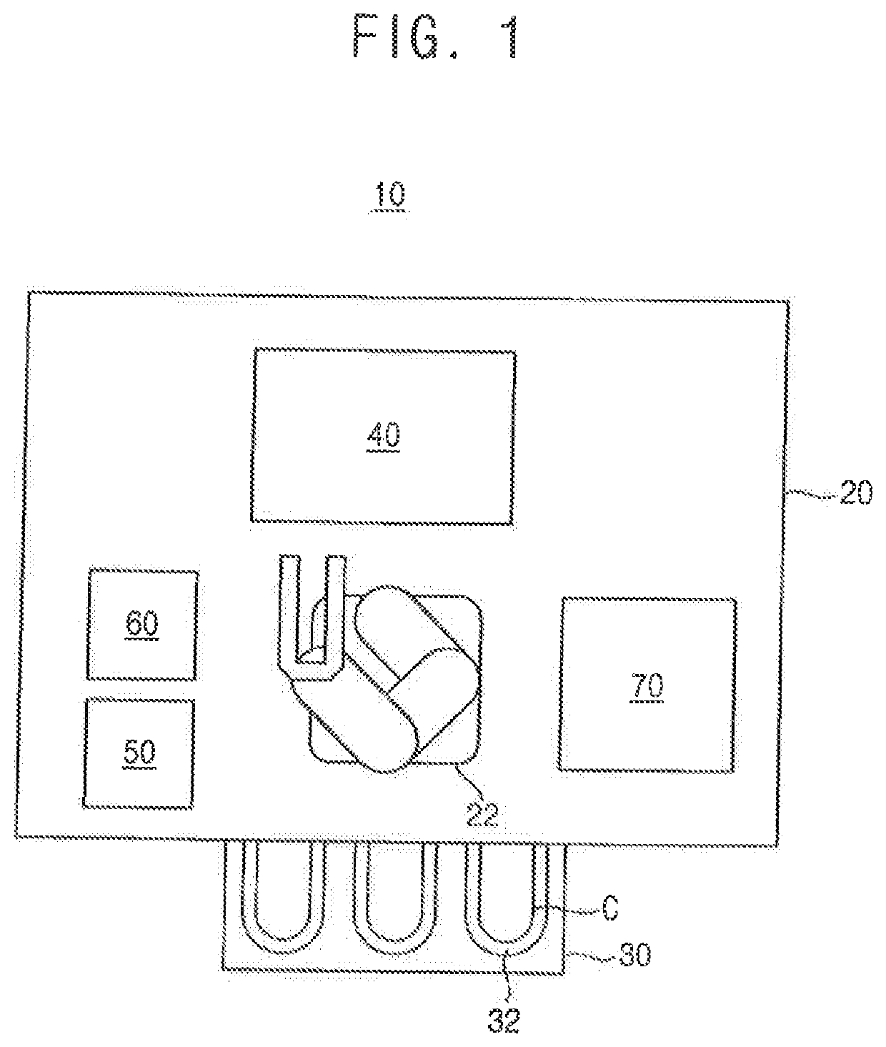
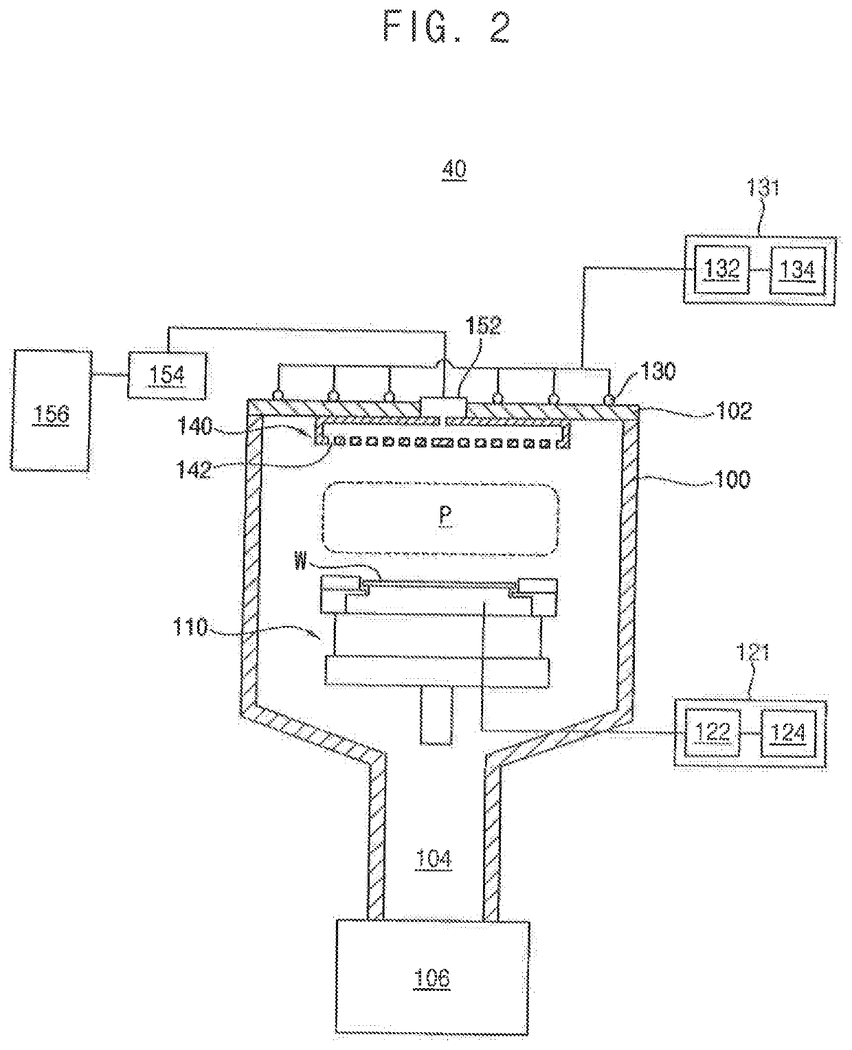
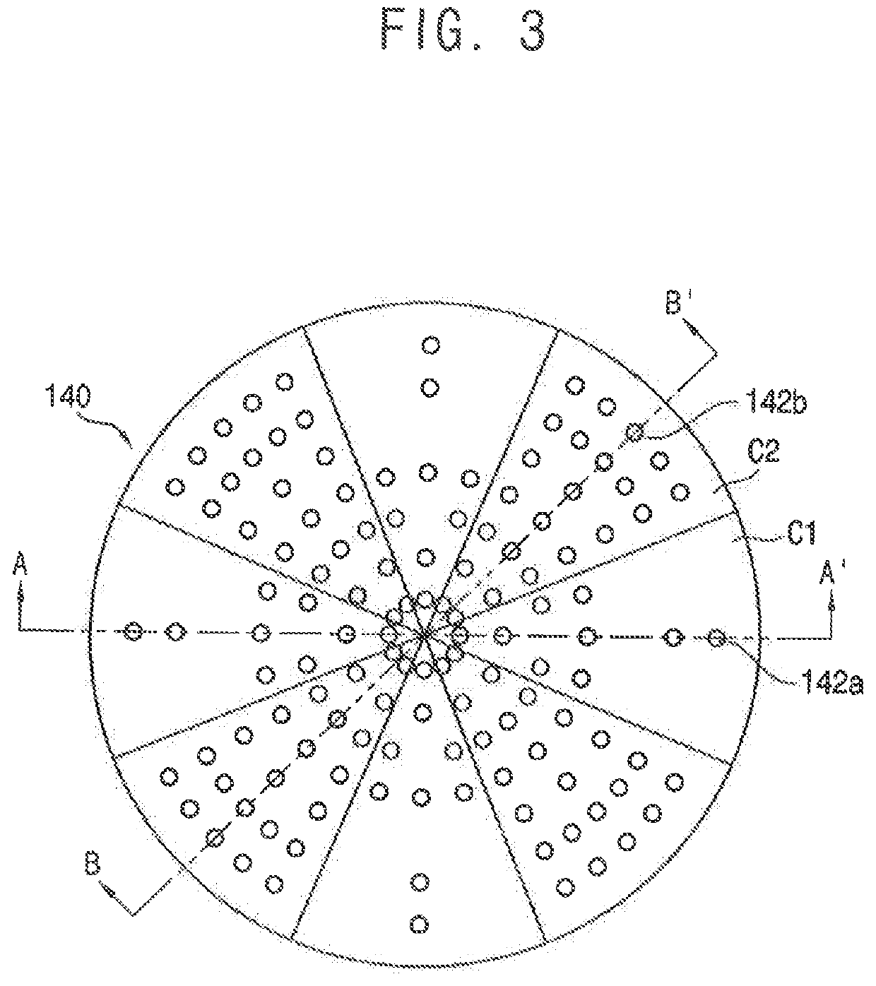
Wafer to wafer bonding method and wafer to wafer bonding system

a bonding system and wafer technology, applied in the direction of solid-state devices, basic electric elements, radiation control devices, etc., can solve the problems of overlay distortion between the bonded wafers, and achieve the effect of preventing wafer to wafer misalignmen

Active Publication Date: 2020-02-06
SAMSUNG ELECTRONICS CO LTD
View PDF0 Cites 0 Cited by
  • Summary
  • Abstract
  • Description
  • Claims
  • Application Information

AI Technical Summary

Benefits of technology

[0004]Exemplary embodiments provide a wafer to wafer bonding method capable of preventing wafer to wafer misalignment.

Problems solved by technology

When the two wafers are bonded to each other in the wafer bonding step, an overlay distortion may occur between the bonded wafers.

Method used


Image

  • Wafer to wafer bonding method and wafer to wafer bonding system
  • Wafer to wafer bonding method and wafer to wafer bonding system
  • Wafer to wafer bonding method and wafer to wafer bonding system

Examples


Embodiment Construction

[0024]Exemplary embodiments will be described more fully hereinafter with reference to the accompanying drawings. Like reference numerals may refer to like elements throughout the accompanying drawings.

[0025]Spatially relative terms, such as “beneath”, “below”, “lower”, “under”, “above”, “upper”, etc., may be used herein for ease of description to describe one element or feature's relationship to another element(s) or feature(s) as illustrated in the figures. It will be understood that the spatially relative terms are intended to encompass different orientations of the device in use or operation in addition to the orientation depicted in the figures. For example, if the device in the figures is turned over, elements described as “below” or “beneath” or “under” other elements or features would then be oriented “above” the other elements or features. Thus, the exemplary terms “below” and “under” can encompass both an orientation of above and below.

[0026]The term “about” as used herein...


PUM

PropertyMeasurementUnit
central angleaaaaaaaaaa
angleaaaaaaaaaa
densitiesaaaaaaaaaa

Abstract

A wafer to wafer bonding method includes performing a plasma process on a bonding surface of a first wafer, pressurizing the first wafer after performing the plasma process on the bonding surface of the first wafer, and bonding the first wafer to a second wafer. The plasma process has different plasma densities along a circumferential direction about a center of the first wafer. A middle portion of the first wafer protrudes after pressurizing the first wafer. The first wafer is bonded to the second wafer by gradually joining the first wafer to the second wafer from the middle portion of the first wafer to a peripheral region of the first wafer.

Description

CROSS-REFERENCE TO RELATED APPLICATIONS[0001]This application claims priority under 35 U.S.C. § 119 to Korean Patent Application No. 10-2018-0090872, filed on Aug. 3, 2018 in the Korean Intellectual Property Office (KIPO), the disclosure of which is incorporated by reference herein in its entirety.TECHNICAL FIELD[0002]Exemplary embodiments relate to a wafer to wafer bonding method and a wafer to wafer bonding apparatus. More particularly, exemplary embodiments relate to method of bonding wafers to each other to manufacture a semiconductor device having a three-dimensional connection structure, and a wafer to wafer bonding apparatus for performing the same.DISCUSSION OF THE RELATED ART[0003]In manufacturing electronic products such as a CMOS image sensor (CIS), High Bandwidth Memory (HBM), etc., two wafers may be bonded to each other, thereby improving a yield rate per wafer. The wafer to wafer bonding process may include an O2 plasma activation step, a hydration step, a wafer alignm...

Claims


Application Information

Patent Timeline
Patent Type & Authority Applications(United States)
IPC IPC(8): H01L23/00H01L21/67H01J37/32H01L25/00H01L25/18H01L27/146H01L21/68H01L23/544
CPCH01L27/14634H01L27/1469H01L2223/54426H01L21/6704H01L2223/54493H01J37/32899H01J37/3244H01L24/75H01L21/67098H01L2224/83031H01J2237/334H01L2224/75753H01J37/32715H01L21/68H01L23/544H01L2224/753H01L21/67069H01L21/67207H01J37/321H01L2224/7501H01L29/045H01L24/83H01L21/67167H01L2224/7555H01L21/6719H01L2224/83203H01L2224/8313H01L21/6838H01L25/18H01L21/67092H01L2224/75744H01L2224/83091H01L25/50H01L2224/83022H01L21/187H01L21/3065H01L24/94H01L2224/94H01L24/80H01L2224/80013H01L2224/80201H01L2224/80948H01L2224/75745H01L24/08H01L2224/08145H01L2224/80H01L2924/00012
Inventor LEE, JOON-HOKIM, SUNG-HYUPSOHN, KI-JU
Owner SAMSUNG ELECTRONICS CO LTD
Why Eureka
Try Eureka