Wafer to wafer bonding apparatuses

a wafer and wafer technology, applied in electrical devices, semiconductor devices, semiconductor/solid-state device details, etc., to achieve the effect of improving the performance, reliability and/or efficiency of said semiconductor devices, reducing or minimizing alignment errors

Active Publication Date: 2022-09-13
SAMSUNG ELECTRONICS CO LTD
View PDF15 Cites 1 Cited by
  • Summary
  • Abstract
  • Description
  • Claims
  • Application Information

AI Technical Summary

Benefits of technology

[0004]Some example embodiments provide a wafer to wafer bonding method capable of preventing wafer to wafer misalignment.
[0009]Thus, while the bonding of the upper wafer and the lower wafer propagates, curvatures of the wafers at adhesion points may be controlled to be symmetric to each other to thereby reduce or minimize an alignment error between the wafers, thereby improving the quality of semiconductor devices formed via such bonding, including improving the performance, reliability, and / or efficiency of said semiconductor devices.

Problems solved by technology

Since in the wafer bonding step, a middle region of the wafer may be deformed to protrude and then may be joined gradually from the middle region to a peripheral region, the wafers may be deformed due to self-weight during bonding propagation of the wafers, such that curvatures of the wafers at adhesion points are asymmetric to each other, thereby causing an alignment error.

Method used


Image

  • Wafer to wafer bonding apparatuses
  • Wafer to wafer bonding apparatuses
  • Wafer to wafer bonding apparatuses

Examples


Embodiment Construction

[0026]Hereinafter, some example embodiments will be explained in detail with reference to the accompanying drawings.

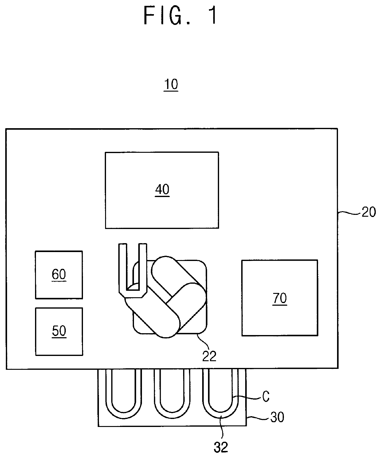
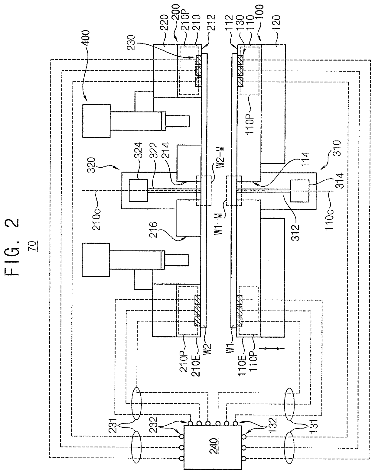
[0027]FIG. 1 is a block diagram illustrating a wafer to wafer bonding system according to some example embodiments.

[0028]Referring to FIG. 1, a wafer to wafer bonding system 10 may include a pre-treatment apparatus such as a plasma processing apparatus 40 and a cleaning apparatus 50, an aligning apparatus 60, and a wafer bonding apparatus 70 arranged in a clean room 20. The wafer to wafer bonding system 10 may further include a cassette stage 30 disposed in a side of the clean room 20.

[0029]In some example embodiments, the clean room 20 may be an enclosed room having a cuboid shape, and may be a controlled environment that has a low level of pollutants such as, for example, dust, airborne microbes, aerosol particles, and chemical vapors.

[0030]The cassette stage 30 may provide a space in which wafers are located before being transferred into the clean room 20. A carrier...


PUM

PropertyMeasurementUnit
outer radiusaaaaaaaaaa

Abstract

A wafer bonding apparatus includes lower and upper stages, lower and upper push rods, a position detection sensor, and processing circuitry. The stages may vacuum suction respective wafers on respective surfaces of the stages based on a vacuum pressure being supplied to respective suction holes in the respective surfaces from a vacuum pump. The push rods are movable through respective center holes in the stages to apply pressure to respective middle regions of the respective wafers. The position detection sensor may generate information indicating a bonding propagation position of the wafers based on detecting at least one wafer through a detection hole in at least one stage. The processing circuitry may process the information to detect the bonding propagation position and cause a change of at least one of a ratio of protruding lengths of the push rods, or a ratio of suction areas of the stages.

Description

CROSS-REFERENCE TO RELATED APPLICATION[0001]This application claims priority under 35 U.S.C. § 119 to Korean Patent Application No. 10-2019-0079283, filed on Jul. 2, 2019 in the Korean Intellectual Property Office (KIPO), the contents of which are herein incorporated by reference in their entirety.BACKGROUND1. Field[0002]Some example embodiments relate to wafer to wafer bonding methods and wafer to wafer bonding apparatuses. More particularly, some example embodiments relate to methods of bonding wafers to each other to manufacture a semiconductor device having a three-dimensional connection structure and wafer to wafer bonding apparatuses for performing the same.2. Description of the Related Art[0003]In manufacturing electronic products such as CIS (CMOS image sensor), HBM (High Bandwidth Memory), etc., two wafers may be bonded to each other, thereby improving a yield rate per wafer. The wafer to wafer bonding process may include an O2 plasma activation step, a hydration step, a wa...

Claims


Application Information

Patent Timeline
Patent Type & Authority Patents(United States)
IPC IPC(8): H01L21/67H01L21/683H01L23/00H01L21/20
CPCH01L21/67092H01L21/2007H01L21/67253H01L21/67259H01L21/6838H01L24/75H01L2224/75744H01L2224/75745H01L2224/808H01L21/68H01L21/681H01L21/185H01L24/80H01L2224/94H01L2224/75901H01L2224/7501H01L2224/80013H01L2224/75802H01L2224/75804H01L2224/75701H01L2224/75702H01L2224/75753H01L2224/8013H01L2224/80132H01L24/94H01L2224/80908H01L2224/80009H01L2224/80986H01L2224/80001H01L2924/00012H01L24/27H01L24/28H01L24/03H01L24/04
Inventor LIM, KYEONGBINYUN, HYEONJUNJO, GWANGHEELEE, JEWONHAN, MINSOOKIM, JUNHYUNGSEOK, SEUNGDAE
Owner SAMSUNG ELECTRONICS CO LTD
Why Eureka
Try Eureka