Image Sensor for Sensing LED Light with Reduced Flickering

a technology of led light and image sensor, which is applied in the field of semiconductor integrated circuits, can solve problems such as unsatisfactory in every aspect, visual disorientation, and danger for light sources that also have a pulsing nature, and achieve the effect of reducing the risk of pulsing

Active Publication Date: 2020-03-26
TAIWAN SEMICON MFG CO LTD
View PDF36 Cites 2 Cited by
  • Summary
  • Abstract
  • Description
  • Claims
  • Application Information

AI Technical Summary

Problems solved by technology

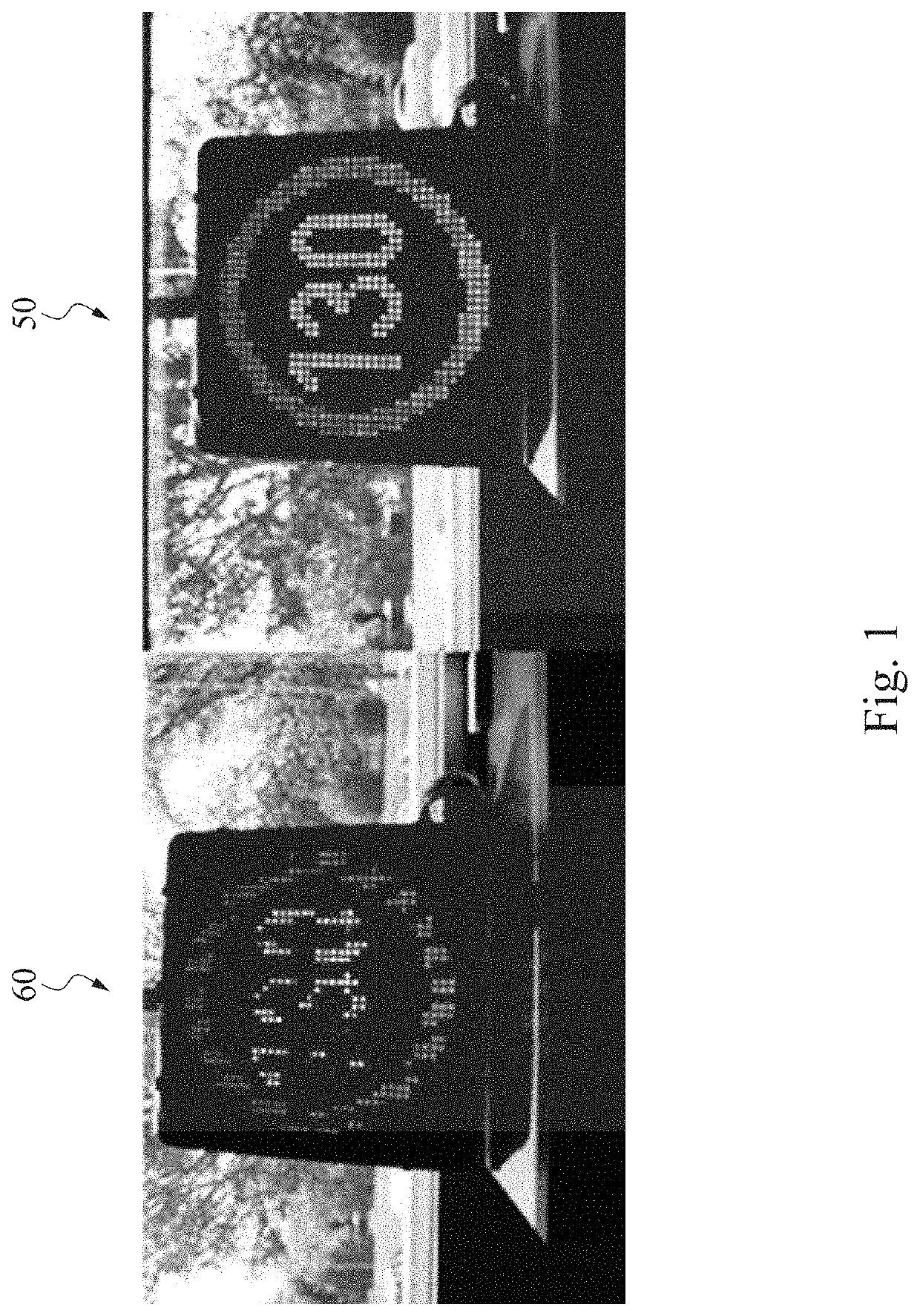
While this type of operation is fine in most situations, it may present a problem with respect to light sources that also have a pulsing nature.
When the flickering effect is produced, it is not only visually displeasing but could also be dangerous, for example in automotive applications where

Method used


Image

  • Image Sensor for Sensing LED Light with Reduced Flickering
  • Image Sensor for Sensing LED Light with Reduced Flickering
  • Image Sensor for Sensing LED Light with Reduced Flickering

Examples


Embodiment Construction

[0013]The following disclosure provides many different embodiments, or examples, for implementing different features of the provided subject matter. Specific examples of components and arrangements are described below to simplify the present disclosure. These are, of course, merely examples and are not intended to be limiting. For example, the formation of a first feature over or on a second feature in the description that follows may include embodiments in which the first and second features are formed in direct contact, and may also include embodiments in which additional features may be formed between the first and second features, such that the first and second features may not be in direct contact. In addition, the present disclosure may repeat reference numerals and / or letters in the various examples. This repetition is for the purpose of simplicity and clarity and does not in itself dictate a relationship between the various embodiments and / or configurations discussed.

[0014]F...


PUM


Abstract

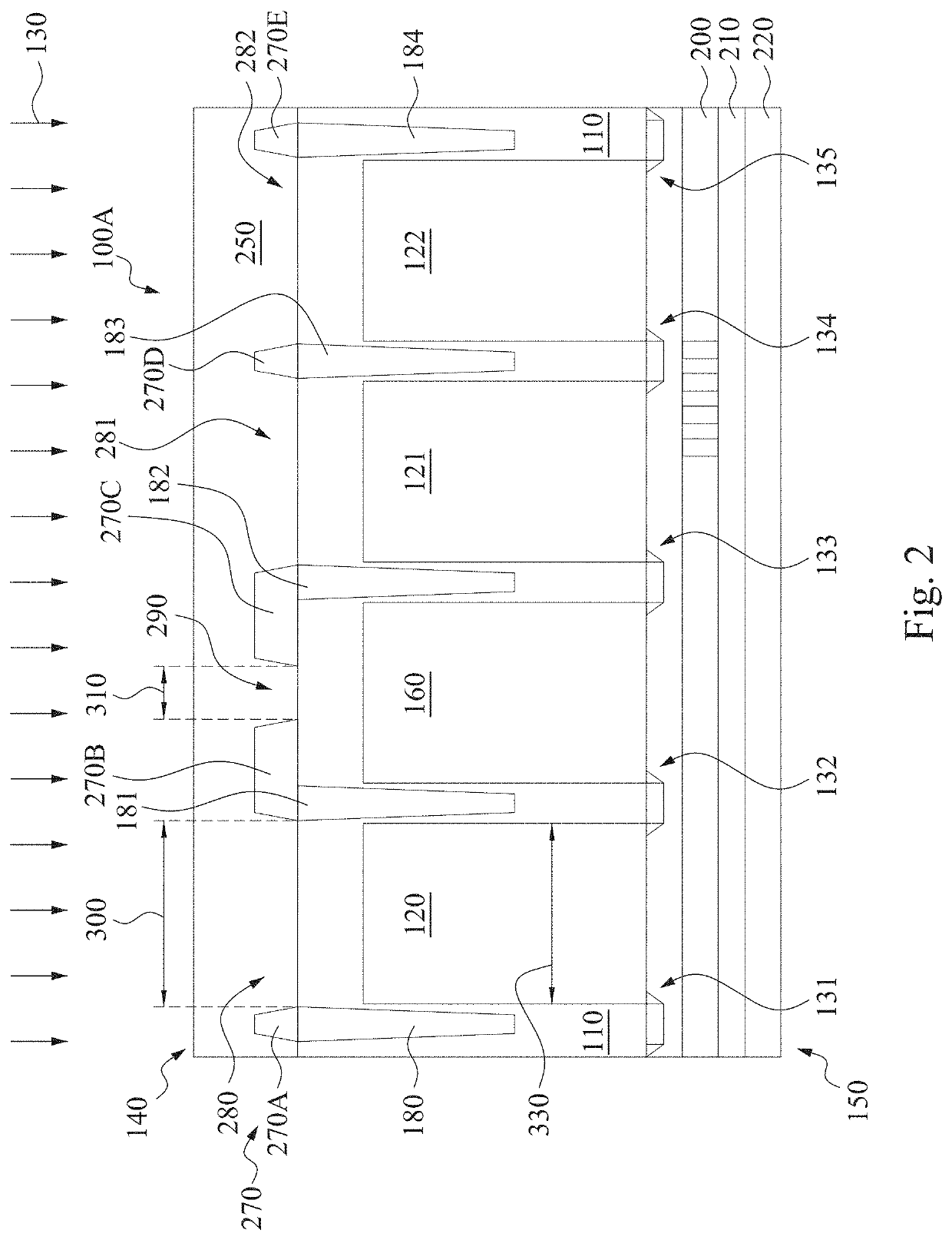
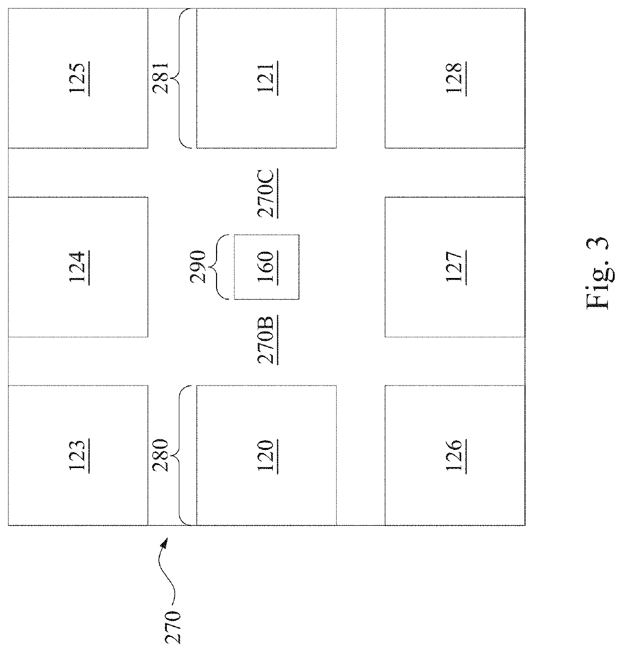
An image sensor device has a first number of first pixels disposed in a substrate and a second number of second pixels disposed in the substrate. The first number is substantially equal to the second number. A light-blocking structure disposed over the first pixels and the second pixels. The light-blocking structure defines a plurality of first openings and second openings through which light can pass. The first openings are disposed over the first pixels. The second openings are disposed over the second pixels. The second openings are smaller than the first openings. A microcontroller is configured to turn on different ones of the second pixels at different points in time.

Description

PRIORITY DATA[0001]This application is a utility application of Provisional U.S. Application No. 62 / 735,886, filed Sep. 25, 2018, which is herein incorporated by reference in its entirety.BACKGROUND[0002]The semiconductor integrated circuit (IC) industry has experienced rapid growth. Technological advances in IC materials and design have produced generations of ICs where each generation has smaller and more complex circuits than the previous generation. Among other applications, semiconductor ICs may be used to implement image sensors to sense radiation such as light. For example, complementary metal-oxide-semiconductor (CMOS) image sensors (CIS) and charge-coupled device (CCD) sensors are widely used in various applications such as digital still camera or mobile phone camera applications. These devices utilize an array of pixels (which may include photodiodes and transistors) in a substrate to absorb (i.e., sense) radiation that is projected toward the substrate and convert the sen...

Claims


Application Information

Patent Timeline
IPC IPC(8): H04N5/235H01L27/146
CPCH04N5/2353H01L27/14645H01L27/14605H01L27/1464H01L27/1463H01L27/1461H04N5/2357H01L27/14621H01L27/14623H04N25/70H01L27/14607H01L27/14612H04N23/745H04N25/44H04N25/585H04N25/702H01L27/14625H04N25/40H04N23/73
Inventor CHENG, YUN-WEICHOU, CHUN-HAOLEE, KUO-CHENGCHEN, HSIN-CHI
Owner TAIWAN SEMICON MFG CO LTD
Why Eureka
Try Eureka