Eureka AIR delivers breakthrough ideas for toughest innovation challenges, trusted by R&D personnel around the world.

Touch display device and manufacturing method thereof

Active Publication Date: 2020-04-09
INTERFACE TECH CHENGDU CO LTD +2
View PDF4 Cites 4 Cited by
  • Summary
  • Abstract
  • Description
  • Claims
  • Application Information

AI Technical Summary

Benefits of technology

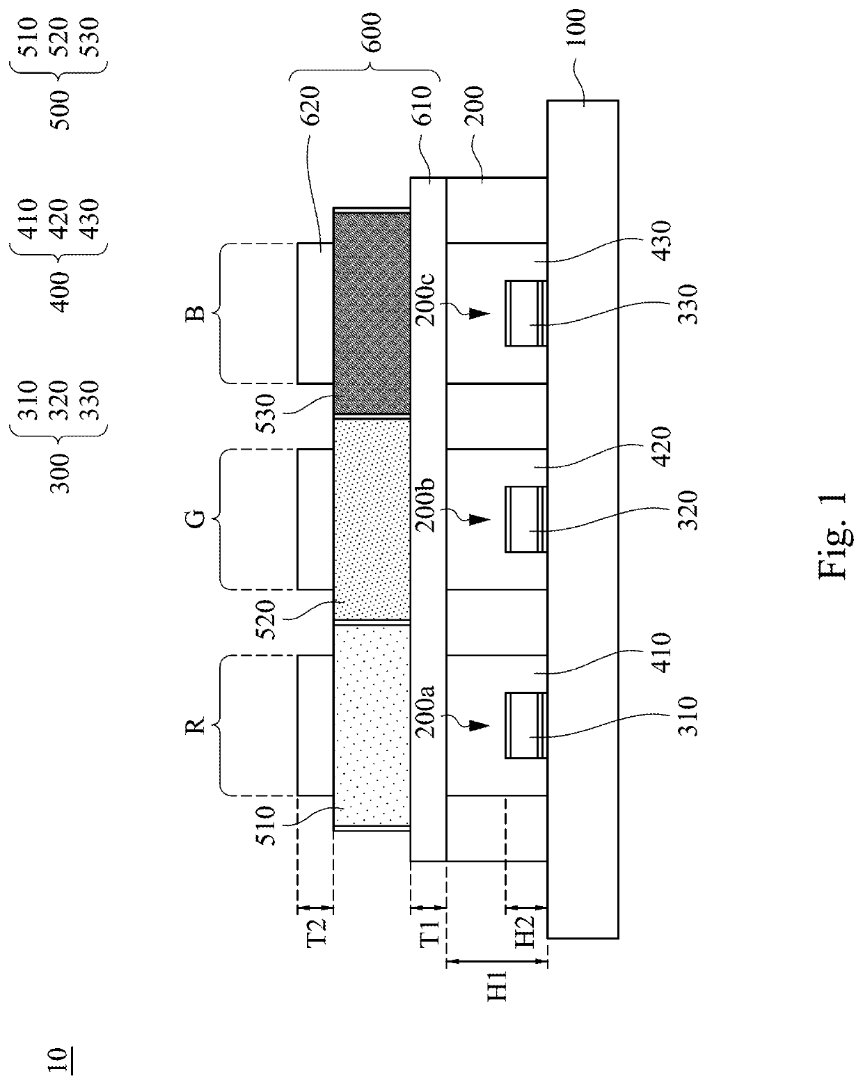
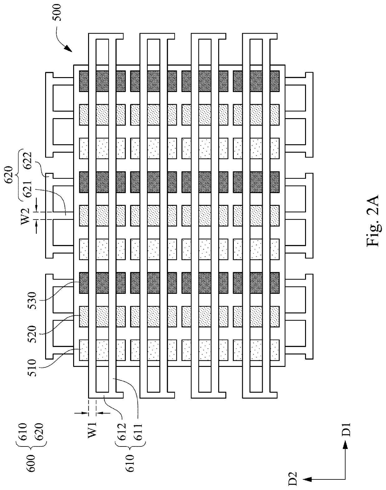
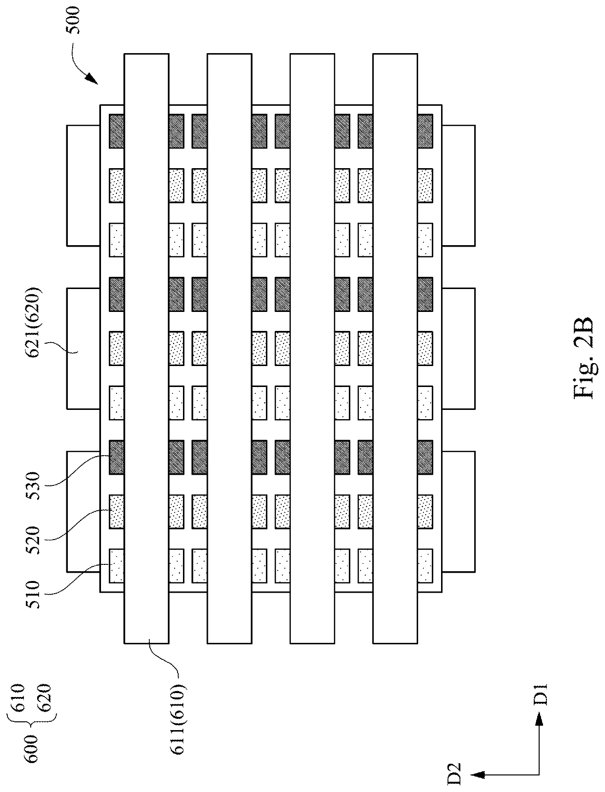
The present invention provides a touch display device comprising a substrate, a light shielding array, a plurality of light emitting elements, a color filter, and a touch control module, wherein the light shielding array is disposed on the substrate with a plurality of openings and each of the light emitting elements is disposed in one of the openings. The color filter is disposed over the light shielding array, and the touch control module includes a bottom electrode layer disposed between the light shielding array and the color filter and a top electrode layer disposed on the color filter. A method of manufacturing the touch display device is also provided. The technical effects of this invention include improved display quality, reduced cost, and simplified manufacturing process.

Problems solved by technology

However, the conventional capacitive touch display device is relatively thicker, so it does not comply with the trend of thin electronic devices.
In addition, if the display device has a phosphor powder or a quantum dot material, the ambient light incident from the outside of the device may excite the phosphor powder or the quantum dot material, thereby causing a mura phenomenon.

Method used


Image

  • Touch display device and manufacturing method thereof
  • Touch display device and manufacturing method thereof
  • Touch display device and manufacturing method thereof

Examples


Embodiment Construction

[0022]The following disclosure provides many different embodiments, or examples, for implementing different features of the provided subject matter. Specific examples of components and arrangements are described below to simplify the present disclosure. These are, of course, merely examples and are not intended to be limiting. For example, the formation of a first feature over a second feature in the description that follows may include embodiments in which the first and second features are formed in direct contact, and may also include embodiments in which additional features are disposed between the first and second features, such that the first and second features are not in direct contact. For the purpose of simplicity and clarity, different features may be depicted with different sizes.

[0023]Further, spatially relative terms, such as “beneath,”“below,”“lower,”“above,”“upper” and the like, may be used herein for ease of description to describe one element or feature's relationsh...


PUM


Abstract

A touch display device includes a substrate, a light shielding array, a plurality of light emitting elements, a color filter, and a touch control module. The light shielding array is disposed on the substrate, and the light shielding array has a plurality of openings. Each of the light emitting elements is placed in one of the openings. The color filter is disposed over the light shielding array. The touch control module includes a bottom electrode layer disposed between the light shielding array and the color filter and a top electrode layer disposed on the color filter.

Description

CROSS-REFERENCE TO RELATED APPLICATION[0001]This application claims priority to China Application Serial Number 201811167625.1, filed Oct. 8, 2018, which is herein incorporated by reference.BACKGROUNDField of Invention[0002]The present invention relates to a touch display device, and a manufacturing method of the touch display device.Description of Related Art[0003]In a conventional capacitive touch display device, the upper and lower touch electrode layers of the touch control module are formed on opposite sides of a transparent substrate. The touch control module is attached to a display device (e.g., a micro light emitting diode (LED) display device), a polarization plate or a cover plate to form the capacitive touch display device.[0004]However, the conventional capacitive touch display device is relatively thicker, so it does not comply with the trend of thin electronic devices. In addition, if the display device has a phosphor powder or a quantum dot material, the ambient ligh...

Claims


Application Information

Patent Timeline
IPC IPC(8): G06F3/041H01L25/075H01L33/58H01L33/56H01L33/50G06F3/044
CPCG06F2203/04103H01L2933/0091G06F3/0412H01L33/56H01L25/0753H01L2933/0058H01L2933/0041H01L33/58H01L2933/005G06F3/044H01L33/502G06F3/0416G06F3/0445G06F3/0446H01L33/44H01L33/504H01L33/54H01L2933/0025
Inventor CHEN, YU-JU
Owner INTERFACE TECH CHENGDU CO LTD
Why Eureka
Eureka Blog
Learn More