Solid State imaging device and method for producing the same

a technology of solid-state imaging and imaging device, which is applied in the direction of instruments, television systems, and details of the television system, can solve the problems of reducing the light receiving area, the reduction of the photoelectric conversion characteristic (photosensitivity), and the conventional techniques cannot meet such severe demands as the reduction of film thickness and miniaturization and dimensional accuracy of the color filter layer, and achieves superior spectral characteristics, high light collection efficiency, and superior durability.

Inactive Publication Date: 2006-08-24
PANASONIC CORP
View PDF3 Cites 53 Cited by
  • Summary
  • Abstract
  • Description
  • Claims
  • Application Information

AI Technical Summary

Benefits of technology

[0038] In view of the above problems, an objective of the present invention is to provide a solid state imaging device which has a color filter including at least two color filter layers with no pattern misalignment but with excellent spectral characteristics and durability, wherein color mixture between adjacent pixels, nonuniform tone of lines, uneven color, etc., are eliminated. Another objective of the present invention is to provide a method for stably producing such a solid state imaging device.

Problems solved by technology

However, such demands on the solid state imaging device result in a reduction of the light receiving area (the area of a photodetection sensor) of a photoelectric conversion element, which constitutes a cause of the decrease in the photoelectric conversion characteristic (photosensitivity) which is a primary characteristic of the solid state imaging device.
Thus, conventional techniques cannot follow such severe demands as to reduction in film thickness and miniaturization and dimensional accuracy of a color filter layer.
Accordingly, the characteristics of the color imaging device are deteriorated due to the color filter layer, so that color mixture, uneven color, nonuniform tone of lines, black defects, etc., occur.
Therefore, the size reduction and the increase in the number of pixels cannot be simultaneously achieved without a decrease in pixel size.
Thus, a decrease in photosensitivity cannot be avoided.
The reduction of the pixel size (miniaturization) causes not only deterioration in photosensitivity but also deteriorations in various color characteristics due to a color filter layer.
That is, in general, the dimensional accuracy of the color filter layer deteriorates along with a decrease in pixel size, and therefore, the characteristics of the solid state imaging device are deteriorated so that color mixture between adjacent pixels, nonuniform tone of lines, variation in photosensitivity, uneven color, etc., occur.
Further, since the dye itself is not in the form of particles, the frequency of occurrences of black defects is low when such a dye-type material is used for a color filter layer.
A disadvantage of the dye-type color filter layer is the necessity for a thicker film for the purpose of achieving desired spectral characteristics.
Because of this, the definition is deteriorated, and this is disadvantageous in finer pattern formation.
However, the colorant which determines the spectral characteristics is in the form of particles, and therefore, the number of black defects is nonnegligibly large as a result of the decrease in pixel size, as to which the pigment-dispersed color filter is inferior to the dye-type color filter.
However, the dye-contained type color filter layer is inferior to the pigment-dispersed color filter layer in readiness to reduce the film thickness and durability (lightfastness, heat resistance, chemical resistance, etc.).
However, none of these color filter layers overcomes all the disadvantages.
However, the above-described conventional technique has other disadvantages as described below.
Since the exposure step is performed twice, the possibility of mask misalignment is increased.
Accordingly, it is difficult to perform pattern formation with a precision desired for the color filter.
That is, misalignment is likely to occur between the two color filter layers.
As a result, the problems of uneven color, nonuniform tone of lines, color mixture between adjacent pixels, etc., are not sufficiently overcome.
Thus, color mixture due to diagonal incident light increases, and the incident angle dependence deteriorates.

Method used


Image

  • Solid State imaging device and method for producing the same
  • Solid State imaging device and method for producing the same
  • Solid State imaging device and method for producing the same

Examples


Embodiment Construction

[0071] Hereinafter, a solid state imaging device of the present invention and a production method thereof are described.

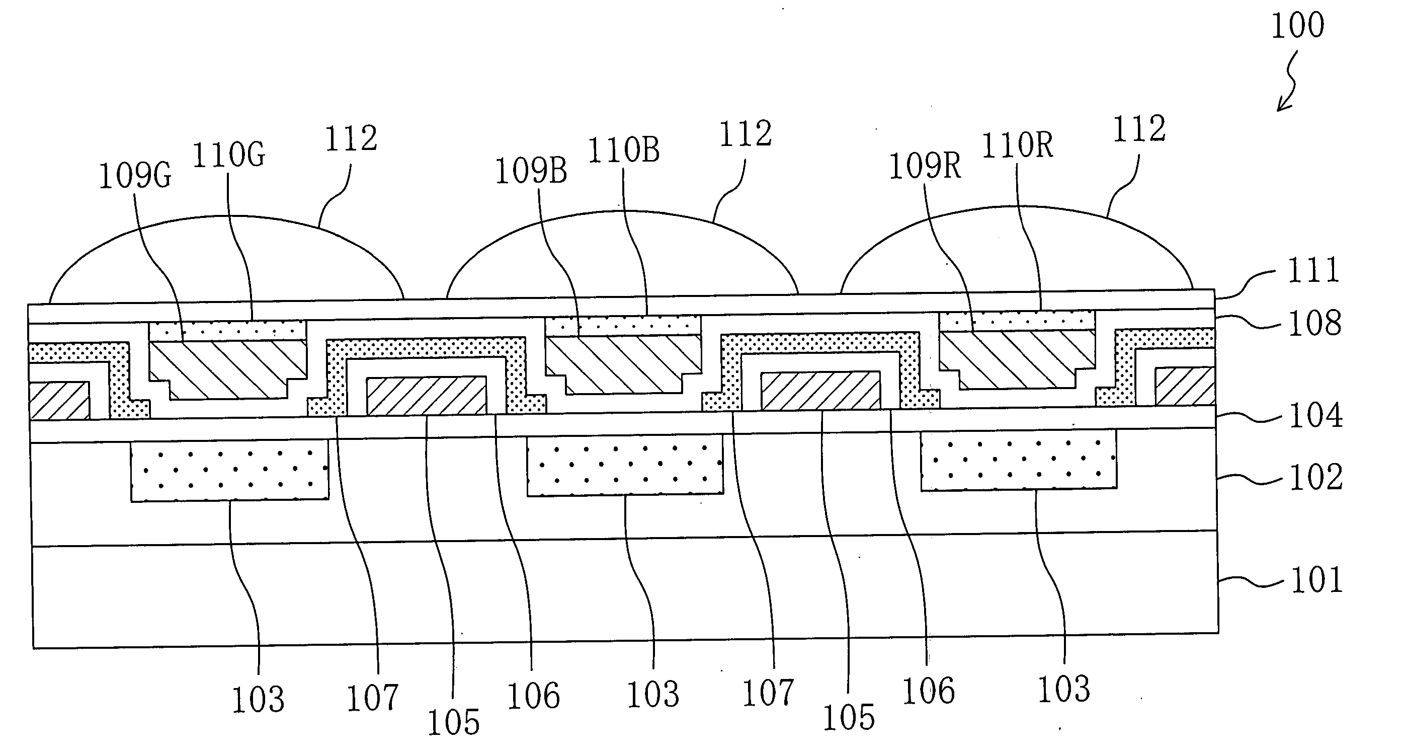
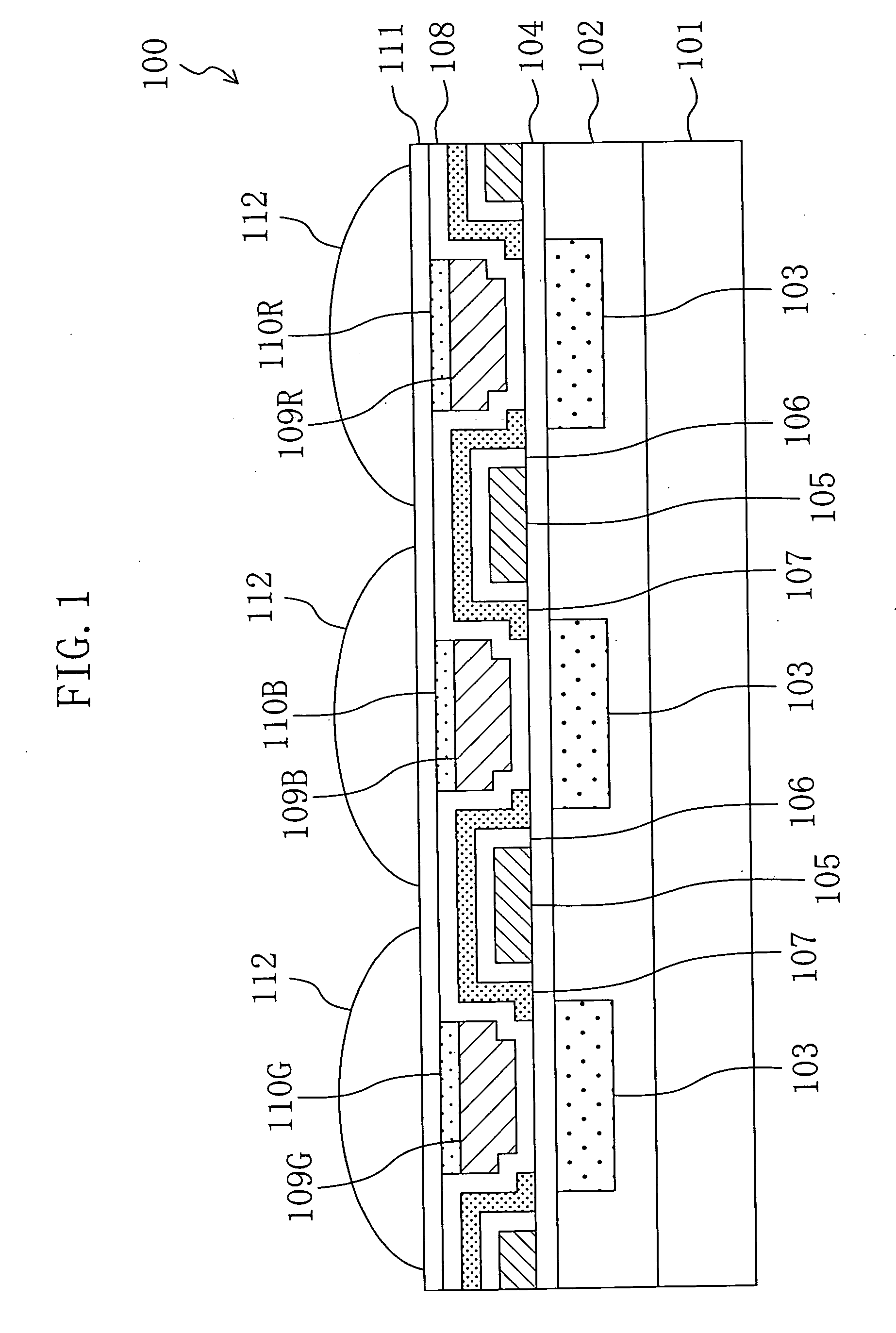
[0072]FIG. 1 schematically shows a cross-sectional structure of a solid state imaging device according to an embodiment of the present invention. FIG. 1 shows an area of three photoelectric conversion elements.

[0073] As shown in FIG. 1, the solid state imaging device 100 of the present invention is herein formed using an N-type semiconductor substrate 101 (semiconductor substrate of the first conductivity type). The solid state imaging device 100 includes a P-type well 102 (second conductivity type well) on the N-type semiconductor substrate 101 and a plurality of photoelectric conversion elements 103 (N-type semiconductor regions) on the P-type well 102. It should be noted that, although not shown, the photoelectric conversion elements 103 are arranged in a matrix over the N-type semiconductor substrate 101. According to the present invention, on the contrary, t...


PUM

PropertyMeasurementUnit
temperatureaaaaaaaaaa
thicknessaaaaaaaaaa
refractive indexaaaaaaaaaa

Abstract

A solid state imaging device comprises a plurality of pixels arranged in a matrix, each of the pixels including: a substrate; a photoelectric conversion element for converting light to electric charges; and a color filter formed on the photoelectric conversion element for color separation. The color filter is a layered color filter including a dye-contained color filter layer and a pigment-dispersed color filter layer formed on the dye-contained color filter layer, the dye-contained color filter layer and the pigment-dispersed color filter layer having the same hue.

Description

CROSS-REFERENCE TO RELATED APPLICATION [0001] This application claims priority under 35 U.S.C. § 119(a) on Japanese Patent Application No. 2005-046811 filed on Feb. 23, 2005, the entire contents of which are hereby incorporated by reference. BACKGROUND OF THE INVENTION [0002] 1. Field of the Invention [0003] The present invention relates to a solid state imaging device which has an on-chip color filter and a method for producing the same. [0004] 2. Description of the Prior Art [0005] In recent years, single-plate color solid state imaging devices has been remarkably developed along with the advancement of color picture imaging. Typical examples of such devices include, for example, a solid state imaging device for digital still cameras, mainly including CCD (Charge Coupled Device)-type devices, and a solid state imaging device for mobile camera phones, mainly including CMOS (Complementary Metal Oxide Semiconductor)-type devices. Therefore, demands for downsizing and increase in the ...

Claims


Application Information

Patent Timeline
Patent Type & Authority Applications(United States)
IPC IPC(8): G02F1/1335H01L27/14H04N5/335H04N5/357H04N5/369
CPCH01L27/14621H01L27/14623H01L27/14627H01L27/14632H01L27/14685H01L27/14687H01L27/14868
Inventor YOKOZAWA, KENJI
Owner PANASONIC CORP
Why Eureka
Try Eureka