Organic EL element and organic EL panel

a technology of organic el elements and organic el panels, applied in the direction of electroluminescent light sources, electric discharge lamps, incensed envelopes/vessels, etc., can solve the problems of unintended colors detected, difficult to achieve sufficient emissivity efficiency for each color, and difficult manufacturing process of panels, so as to reduce the required precision concerning the thickness of the el element portion constituting the microresonator, the effect of reducing the dependence on the viewing angl

Active Publication Date: 2005-04-07
SANYO ELECTRIC CO LTD
View PDF21 Cites 54 Cited by
  • Summary
  • Abstract
  • Description
  • Claims
  • Application Information

AI Technical Summary

Benefits of technology

[0010] According to the present invention, a microresonator (microcavity) is provided in a portion of a pixel having an organic EL element. Light ejected through a semi-transmissive film is thereby limited to a specific wavelength while the specific wavelength is intensified. The light obtained after the wavelength selection by the microresonator is subseque...

Problems solved by technology

However, when employing this method, the panel manufacturing process becomes difficult and complex because measures must be effected to compensate for differences in emissive efficiency of the emissive materials for different colors, and steps for applying different emissive materials to corresponding pixels must be carried out separately.
However, according to these methods, it is difficult to achieve sufficient emissive efficien...

Method used


Image

  • Organic EL element and organic EL panel
  • Organic EL element and organic EL panel
  • Organic EL element and organic EL panel

Examples


Embodiment Construction

[0022] Preferred embodiments of the present invention will next be described referring to the drawings.

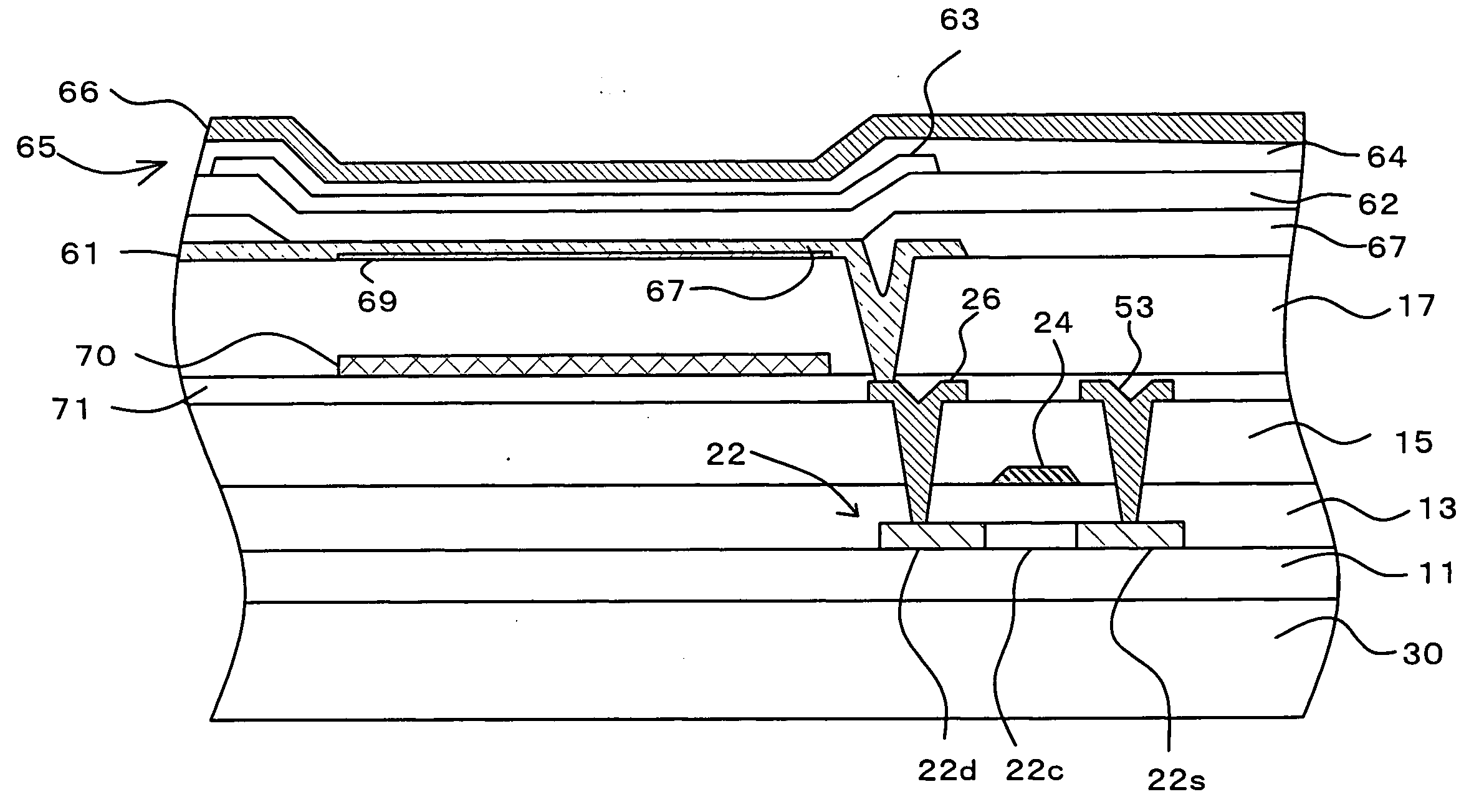
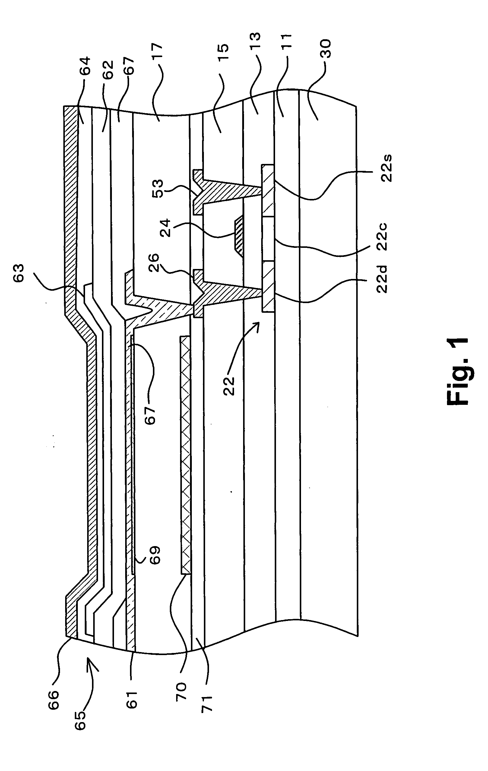
[0023]FIG. 1 is a cross-sectional view showing a configuration of a light-emitting region and a drive TFT (thin film transistor) within one pixel. It should be noted that each pixel actually includes a plurality of TFTs. The drive TFT is the TFT which controls a current supplied from a power line to an organic EL element within the pixel. On a glass substrate 30, a buffer layer 11 composed of a lamination of an SiN layer and an SiO2 layer is formed over the entire surface. Further on top, an active layer 22 made of polysilicon is disposed in predetermined areas (where TFTs are to be created).

[0024] Covering the active layer 22 and the buffer layer 11, a gate insulation film 13 is formed over the entire surface. The gate insulation film 13 may be formed by laminating an SiO2 layer and an SiN layer. On top of the gate insulation film 13 at a position above a channel region 22c, a g...


PUM


Abstract

A semi-transmissive film is provided underneath a transparent electrode of an organic EL element. The optical length of the interval between the upper surface of the semi-transmissive film and the lower surface of a counter electrode serving as a reflective layer is configured such that this interval functions as a microresonator for selecting light having a specific wavelength. A color filter is provided underneath the semi-transmissive film to further restrict the wavelength of light which has passed through the semi-transmissive film.

Description

CROSS-REFERENCE TO RELATED APPLICATIONS [0001] The priority Japanese applications No. 2003-342665 and No. 2004-275673 upon which this patent application is based is hereby incorporated by reference. BACKGROUND OF THE INVENTION [0002] 1. Field of the Invention [0003] The present invention relates to an organic EL element which comprises a transparent electrode, an organic emissive layer disposed over the transparent electrode, and a counter electrode disposed over the organic emissive layer, and emits light when a voltage is applied between the transparent electrode and the counter electrode. [0004] 2. Description of the Related Art [0005] In recent years, organic electroluminescence (hereinafter referred to as “EL”) displays have gained attention as one type of flat display which would replace liquid crystal displays in the coming generation. In a display panel of an organic EL display (hereinafter referred to as “organic EL panel”), the color of light emitted from each pixel may be...

Claims


Application Information

Patent Timeline
IPC IPC(8): H01L27/32H05B33/12H01L51/50H01L51/52H05B33/00H05B33/14H05B33/22H05B33/24H05B33/26
CPCH01L27/3211H01L51/5265H01L27/3244H01L27/322H10K59/35H10K59/38H10K59/12H10K50/852H05B33/22H05B33/24
Inventor NISHIKAWA, RYUJIOMURA, TETSUJI
Owner SANYO ELECTRIC CO LTD
Why Eureka
Try Eureka