Structure of complementary metal oxide semiconductor image sensor and its manufacturing method

An image sensor and barrier metal layer technology, which is applied in semiconductor/solid-state device manufacturing, semiconductor devices, and semiconductor/solid-state device components, etc., and can solve problems such as impact and unfavorable performance.

Inactive Publication Date: 2004-08-04
SAMSUNG ELECTRONICS CO LTD
View PDF0 Cites 54 Cited by
  • Summary
  • Abstract
  • Description
  • Claims
  • Application Information

AI Technical Summary

Problems solved by technology

However, these materials are opaque and thus adversely affect the performance of imaging devices with photodiodes, which depend entirely on the level of external light received

Method used


Image

  • Structure of complementary metal oxide semiconductor image sensor and its manufacturing method
  • Structure of complementary metal oxide semiconductor image sensor and its manufacturing method
  • Structure of complementary metal oxide semiconductor image sensor and its manufacturing method

Examples


Embodiment Construction

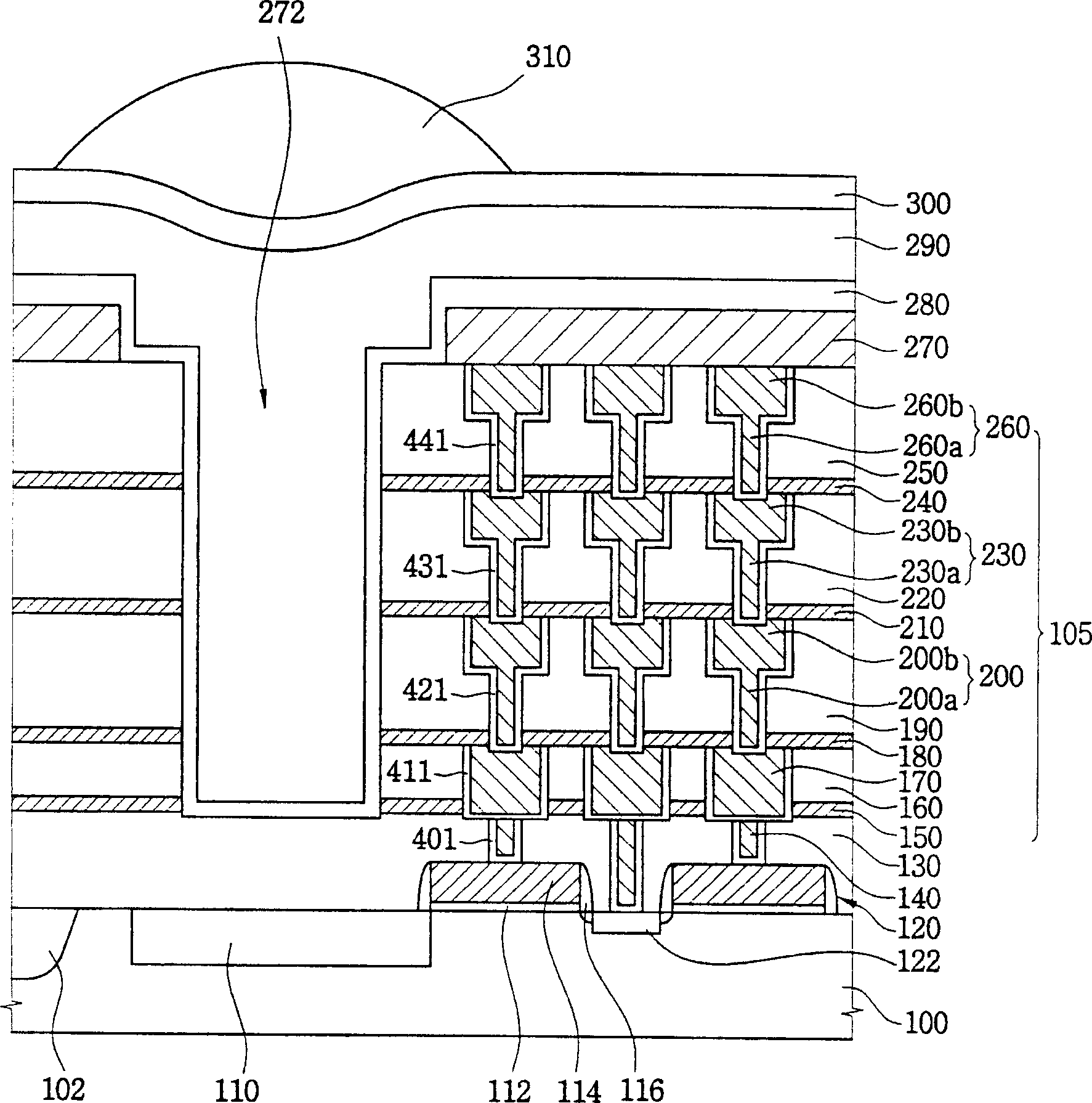
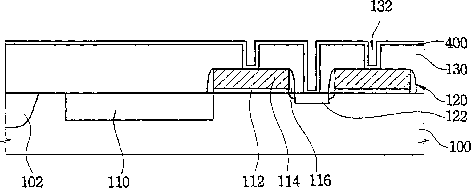
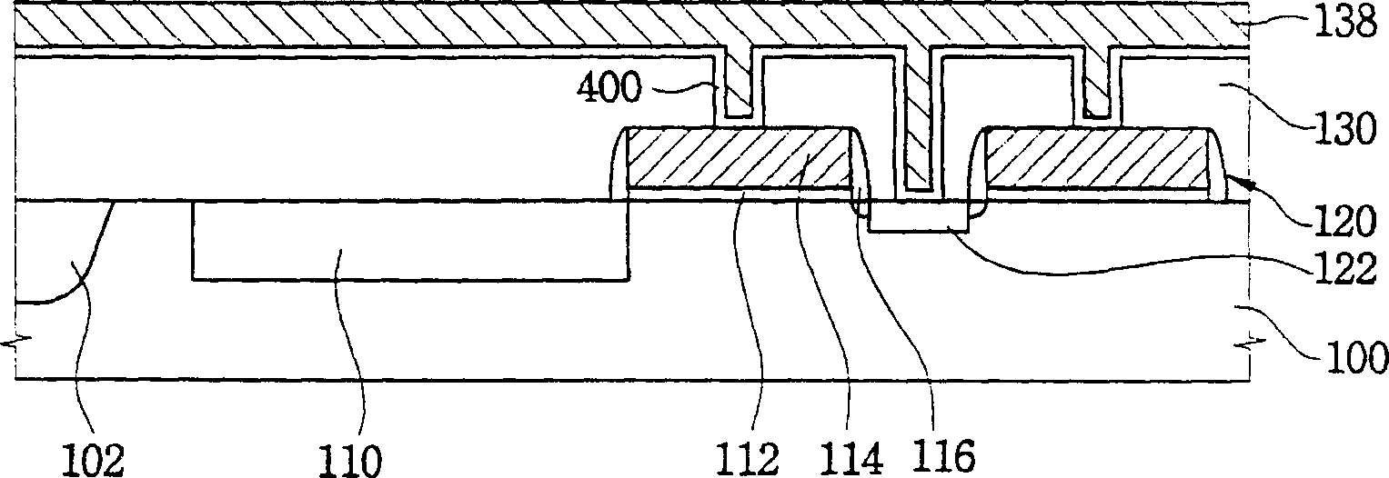
[0026] The invention will now be described more fully with reference to the accompanying drawings, in which preferred embodiments of the invention are shown. However, there may be many implementations of the present invention, and should not be limited to manufacture according to the examples presented herein. However, these embodiments are provided to make the disclosure of this application sufficient and complete, and to fully demonstrate the protection scope of the present invention to those skilled in the art. In the drawings, the thickness of layers and regions are exaggerated for clarity, and the same elements are denoted by the same reference numerals.

[0027] In addition, it is also understood that although embodiments of the present invention are described in connection with p / n type photodiodes, other photodiodes such as PIN type photodiodes and avalanche type photodiodes may also be used.

[0028] In one embodiment of the present invention, there is provided as f...


PUM


Abstract

Structure of a CMOS image sensor and method for fabricating the same. An image sensor device and method for forming the same include a photodiode formed in a substrate, at least one electrical interconnection line electrically associated with the photodiode, a light passageway having a light inlet, the light passageway being positioned in alignment with the photodiode, a color filter positioned over the light inlet of the light passageway and a lens positioned over the color filter in alignment with the light passageway wherein the at least one electrical interconnection line includes a copper interconnection formation having a plurality of interlayer dielectric layers in a stacked configuration with a diffusion barrier layer between adjacent interlayer dielectric layers, and a barrier metal layer between the copper interconnection formation and the plurality of interlayer dielectric layers and intervening diffusion barrier layers. An image sensor device may employ copper interconnections if a barrier metal layer is removed from above a photodiode.

Description

technical field [0001] The invention relates to a structure of a photodiode image sensing device and a manufacturing method thereof. More particularly, the present invention relates to a photodiode image sensing device having copper interconnects and a method of manufacturing the same. Background technique [0002] Photodiode image sensors convert optical information into electrical signals. At present, there are basically two different types of solid-state image sensors: MOS (metal-oxide-semiconductor, metal-oxide-semiconductor) type and CCD (charge coupled device, charge-coupled device) type. Products using photodiodes include those using contact image sensors (CISs), such as hand-held phones (HHPs), cameras, and scanners, including cameras integrated in cell phones. Other products that employ photodiodes include those that rely on charge-coupled devices (CCDs), such as CCTV cameras, camcorders, and digital video cameras. [0003] In recent years, aluminum is commonly u...

Claims


Application Information

Patent Timeline
Patent Type & Authority Applications(China)
IPC IPC(8): H01L21/3205H01L21/768H01L23/52H01L23/522H01L23/532H01L27/14H01L27/146H01L31/0224H04N5/335H04N5/369H04N5/374
CPCH01L27/14625H01L21/76807H01L27/14632H01L21/76801H01L21/76844H01L27/14629H01L31/022408H01L27/14623H01L27/14636H01L21/76843H01L21/76865H01L21/76805H01L27/14685H01L27/14627H01L23/53238H01L2924/0002H01L2924/00
Inventor 李守根朴基彻李敬雨
Owner SAMSUNG ELECTRONICS CO LTD
Why Eureka
Try Eureka