Image sensor and method for manufacturing the same

a technology of image sensor and manufacturing method, which is applied in the direction of electrical equipment, semiconductor devices, radio frequency control devices, etc., can solve the problems of reducing the size of capacitors, deteriorating cis characteristics, and reducing the light signal entering the photodiode region

Active Publication Date: 2010-06-29
INTELLECTUAL DISCOVERY CO LTD
View PDF6 Cites 163 Cited by
  • Summary
  • Abstract
  • Description
  • Claims
  • Application Information

AI Technical Summary

Problems solved by technology

In this case, because the distance from a lens to the photodiode becomes large due to a back-end-of-the-line (BEOL) metal line formed on the transistor region and the capacitor, there is a great loss of the light signal entered into the photodiode region.
Also, according to the related art, because a process is simultaneously performed on the relatively large sized photodiode region and the very small transistor region, a difficulty in a lithography process occurs, which results in many defects occurring, and the photodiode region is attacked in a subsequent process forming a transistor, so that the CIS characteristics would be deteriorated.
Also, according to the related art, as the device becomes smaller using technologies below 90 nm and 65 nm, the size of the capacitor reduces and thus, it becomes more difficult to manufacture the capacitor with a desired capacitance.
Also, according to the related art, since a multi-layer metal line and a capacitor are manufactured together, the distance from a microlens to a photodiode is long, which can result in many problems in manufacturing the microlens.
Also, according to the related art, the transistor region and the capacitor coexist in one CIS device, which results in a region where all of the light incident cannot be absorbed but, rather, is lost.

Method used


Image

  • Image sensor and method for manufacturing the same
  • Image sensor and method for manufacturing the same
  • Image sensor and method for manufacturing the same

Examples


Embodiment Construction

[0017]Hereinafter, an image sensor and a method for manufacturing the same according to embodiments of the present invention will be described in detail with reference to the accompanying drawings.

[0018]In the description of embodiments, it will be understood that when a layer (or film) is referred to as being ‘on’ another layer or substrate, it can be directly on another layer or substrate, or intervening layers may also be present. Further, it will be understood that when a layer is referred to as being ‘under’ another layer, it can be directly under another layer, or one or more intervening layers may also be present. In addition, it will also be understood that when a layer is referred to as being ‘between’ two layers, it can be the only layer between the two layers, or one or more intervening layers may also be present.

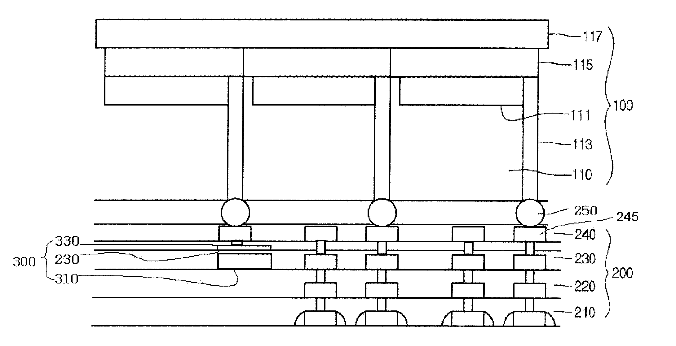
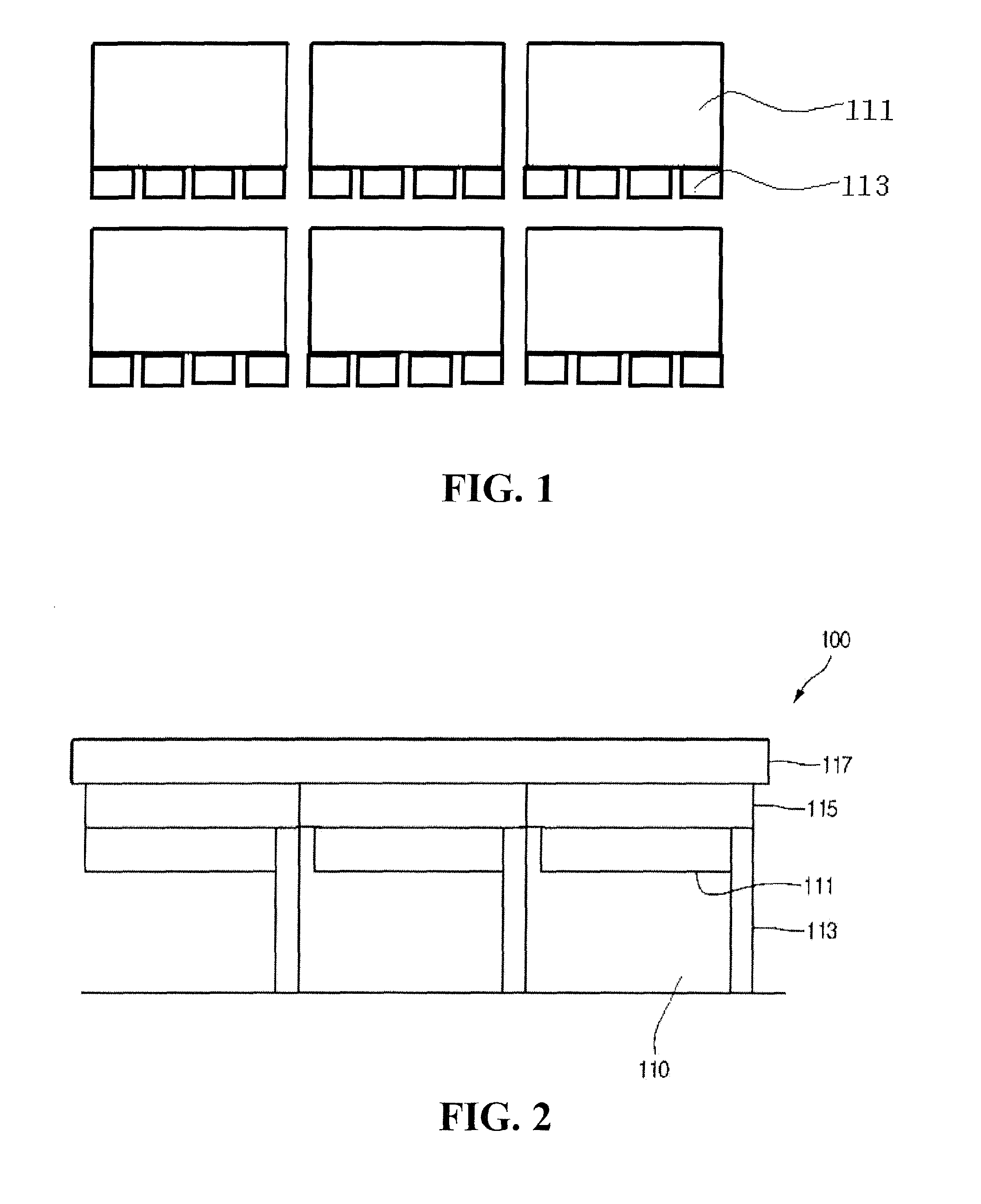
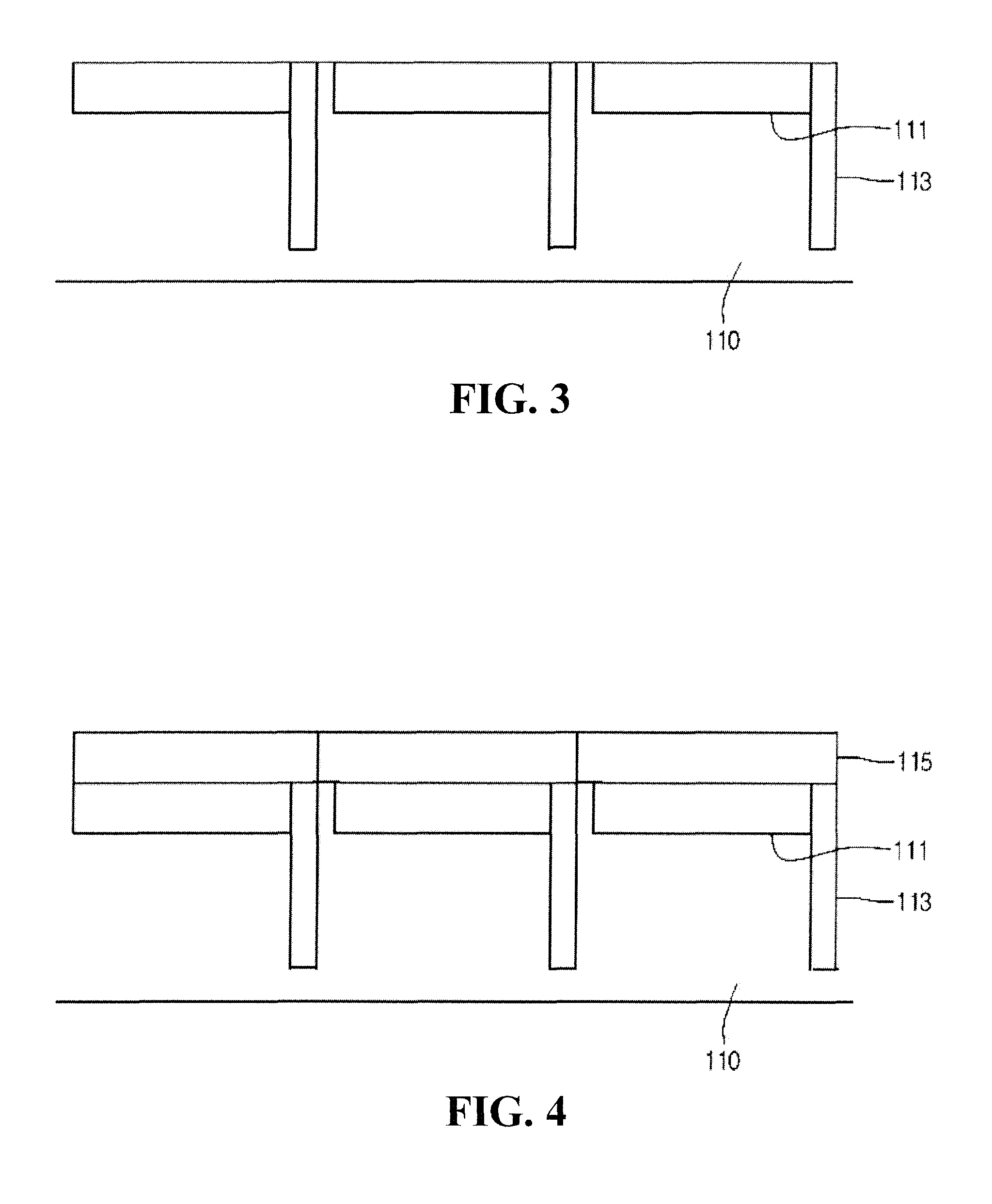
[0019]In an embodiment, an efficient scheme for manufacturing an image sensor is provided. The scheme involves separately manufacturing a first wafer with a phot...


PUM


Abstract

An image sensor and manufacturing process thereof are provided. An image sensor according to an embodiment comprises a first wafer formed with a photodiode cell without a microlens and a second wafer formed with a circuit part including transistor and a capacitor. The first wafer is stacked on the second wafer such that a connecting electrode can be used to electrically connect the photodiode cell of the first wafer to the circuit part of the second wafer.

Description

CROSS-REFERENCE TO RELATED APPLICATION[0001]The present application claims the benefit under 35 U.S.C. §119 of Korean Patent Application No. 10-2006-0135759, filed Dec. 27, 2006, which is hereby incorporated by reference in its entirety.BACKGROUND[0002]In general, an image sensor, which is a semiconductor device converting an optical image into an electrical signal, is typically classified as a charge coupled device (CCD) or a complementary metal oxide silicon (CMOS) image sensor (CIS).[0003]The CIS device according to the related art includes a photodiode region for receiving a light signal and converting it into an electrical signal, and a transistor region for processing the electrical signal.[0004]Also, the CIS device typically needs one or more capacitors per pixel array.[0005]However, according to the related art, the photodiode region, the transistor region, and the capacitor region are implemented on one wafer during the same fabrication process.[0006]In this case, because t...

Claims


Application Information

Patent Timeline
Patent Type & Authority Patents(United States)
IPC IPC(8): H01L29/72
CPCH01L27/1469H01L27/14634H01L27/146
Inventor HAN, JAE WON
Owner INTELLECTUAL DISCOVERY CO LTD
Why Eureka
Try Eureka