Display device and method for driving display device

Inactive Publication Date: 2011-08-25
SEMICON ENERGY LAB CO LTD
View PDF101 Cites 157 Cited by
  • Summary
  • Abstract
  • Description
  • Claims
  • Application Information

AI Technical Summary

Benefits of technology

[0013]According to one embodiment of the present invention, a display device having a touch panel function capable of preventing false re

Problems solved by technology

In such a display device having a photosensor, external light easily affects imaging accuracy.
Within this wide range of illuminance, it is difficult to make a photosensor recognize the contrast uniformly; thus, false recognit

Method used


Image

  • Display device and method for driving display device
  • Display device and method for driving display device
  • Display device and method for driving display device

Examples


embodiment 1

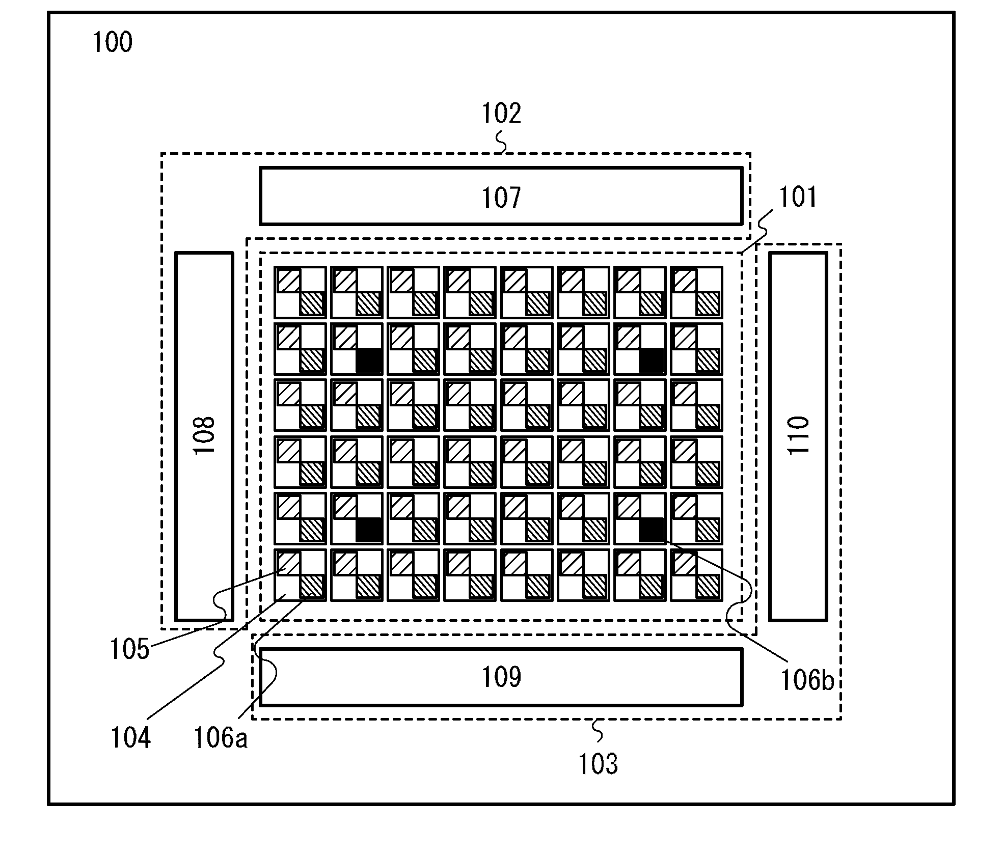
[0032]In this embodiment, a display device according to one embodiment of the present invention will be described with reference to drawings. FIG. 1 illustrates an example of a structure thereof

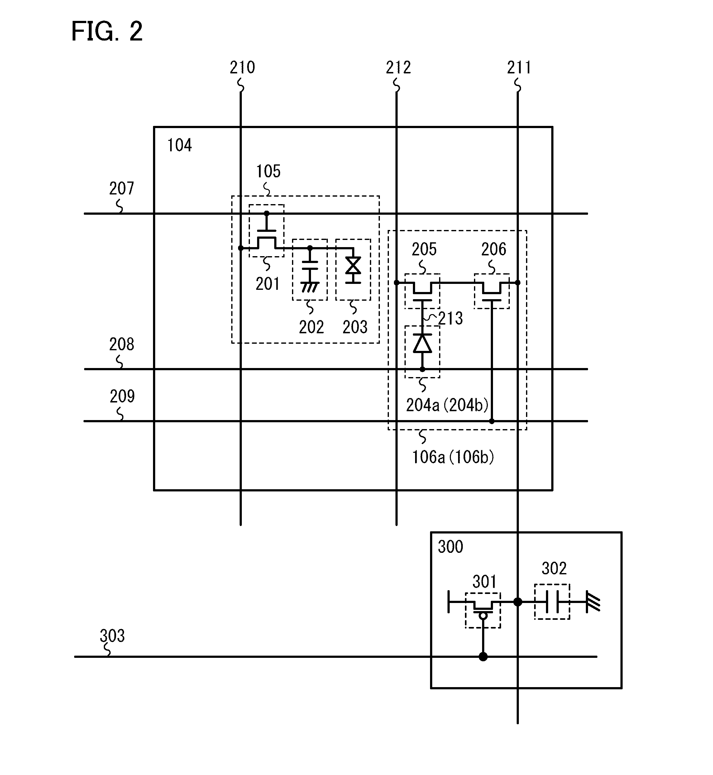
[0033]A display device 100 includes a pixel circuit 101, a display element control circuit 102, and a photosensor control circuit 103. The pixel circuit 101 includes a plurality of pixels 104 arranged in a matrix of rows and columns. Each pixel 104 includes a display element portion 105, and a first photosensor portion 106a or a second photosensor portion 106b, for example.

[0034]The first photosensor portion 106a is provided to obtain an image, and the second photosensor portion 106b is provided mainly to detect the intensity of external light. Note that in some cases, imaging is performed with the second photosensor portion 106b.

[0035]It is not necessary to provide the photosensor portions for all the pixels, and the photosensor portions may be formed in accordance with a purpose. Moreover,...

embodiment 2

[0098]In this embodiment, a method for processing a signal outputted from a photosensor which is mounted on a display device and making the display device function as a touch panel will be described.

[0099]In order that the display device on which a photosensor is mounted recognizes contact on a surface of the display device by a finger, a pen, or the like, it is necessary to image shadows which are caused by shielding external light with the finger, the pen, or the like.

[0100]The shadows are imaged and the position in a display region is recognized in the following manner. First, the target position in the display region is made in contact with a finger or a pen, an imaging operation is performed on the entire display region or part thereof, and thus an image of FIG. 7A is obtained. Next, as illustrated in FIG. 7B, a process for displaying a tone of the shadows with two gray scales is performed, and binary (white and black) determination is performed. Then, the position of the shado...

embodiment 3

[0113]In this embodiment, a liquid crystal display device which is an example of the display device disclosed in this specification will be described.

[0114]FIG. 11 illustrates an example of a cross-sectional view of a liquid crystal display device. In the liquid crystal display device in this embodiment, a photodiode 1002, a transistor 1003a, a transistor 1003b, a transistor 1003c, a storage capacitor 1004, and a liquid crystal element 1005 are provided over a substrate 1001 having an insulating surface. Note that a photosensor and a display element are partly shown on the left side and the right side, respectively, of a short dash line at the center of FIG. 11, and these structures are equivalent to the configuration of the pixel 104 described in Embodiment 1 (see FIG. 2).

[0115]Although a top-gate structure is illustrated as a typical example of the structure of each of the transistor 1003a, the transistor 1003b, and the transistor 1003c, without limitation thereto, another structu...


PUM


Abstract

A display device includes a pixel which includes a first photosensor portion having a first photodiode for detecting visible light, which is provided together with a display element portion; and a pixel which includes a second photosensor portion having a second photodiode for detecting infrared rays, which is provided together with another display element portion. The second photosensor portion detects infrared rays included in external light, and selects an imaging element and adjusts sensitivity in accordance with the amount of infrared rays detected by the second photosensor portion.

Description

TECHNICAL FIELD[0001]Embodiments of the present invention relate to a display device in which pixels each having a photosensor are arranged in a matrix and to a driving method of the display device. Further, an embodiment of the present invention relates to an electronic device including the display device.BACKGROUND ART[0002]In recent years, a display device provided with a sensing element for detecting light (also referred to as a “photosensor”) has attracted attention. A display device having a photosensor in a display region, which can detect a touch of an object to be detected (e.g., a pen and a finger) on the display region, is also called a touch panel, a touch screen, or the like (hereinafter simply called a “touch panel”). Such a photosensor provided in the display region enables the display region to double as an input region; as an example, a semiconductor device having an image loading function has been disclosed in Patent Document 1.[Reference][Patent Document][Patent D...

Claims


Application Information

Patent Timeline
IPC IPC(8): G06F3/038G01J5/10G01J5/20
CPCG01J1/42G01J1/18G01J1/4204G06F3/042G02F1/13318G02F1/1333G09F9/00G09F9/33G09F9/35G09G3/20G09G3/32G09G3/3208G09G3/36H01L27/14603H01L27/14612G06F3/04164G06F3/0325G06F3/0412H01L27/14643G06F2203/04109
Inventor KUROKAWA, YOSHIYUKIIKEDA, TAKAYUKITAMURA, HIKARU
Owner SEMICON ENERGY LAB CO LTD
Why Eureka
Try Eureka