Method for fabricating organic light emitting diode display

a technology of light-emitting diodes and organic materials, applied in the field of displays, can solve the problems of polarizer lamination process, mura, or other defects, reducing the efficiency and life of oled devices, etc., and achieves the effect of improving the uniformity of thickness, compactness and surface lamination performance of thin films, and less prone to mura

Active Publication Date: 2020-07-16
WUHAN CHINA STAR OPTOELECTRONICS SEMICON DISPLAY TECH CO LTD
View PDF3 Cites 1 Cited by
  • Summary
  • Abstract
  • Description
  • Claims
  • Application Information

AI Technical Summary

Benefits of technology

[0045]In the method for fabricating the OLED display in accordance with the present disclosure, the superhydrophobic thin film is formed using the plasma chemical v...

Problems solved by technology

Because organic light emitting polymers in organic light emitting diodes (OLEDs) are easily corroded by oxygen and water, which cause oxidation reactions of organic light emitting polymers, efficiency and lifes of OLED devices are decreased.
Spraying cannot ensure uniformity, which may easily cause...

Method used


Image

  • Method for fabricating organic light emitting diode display

Examples


Embodiment Construction

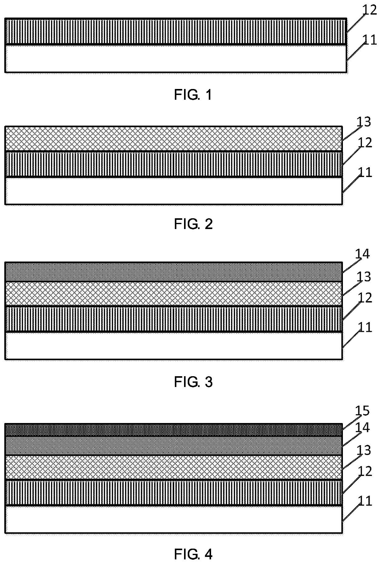
[0050]The description of each embodiment below refers to respective accompanying drawing(s), so as to illustrate exemplarily specific embodiments of the present disclosure that may be practiced. Directional terms mentioned in the present disclosure, such as “upper”, “lower”, “front”, “back”, “left”, “right”, “inner”, “outer”, “side”, etc., are only directions by referring to the accompanying drawings, and thus the used directional terms are used to describe and understand the present disclosure, but the present disclosure is not limited thereto. In the drawings, structurally similar units are labeled by the same reference numerals.

[0051]Referring to FIGS. 1 to 4, FIG. 1 is a schematic structural diagram of a first step of a method for fabricating an organic light emitting diode (OLED) display in accordance with the present disclosure.

[0052]As illustrated in FIGS. 1 to 4, the method for fabricating the OLED display in accordance with the present disclosure mainly includes the followi...


PUM


Abstract

A method for fabricating an organic light emitting diode (OLED) display is provided. The fabricating method includes: forming a switch array layer on a base substrate; forming an organic light emitting display layer on the switch array layer; forming a thin film package layer on the organic light emitting display layer; and forming a superhydrophobic thin film on the thin film package layer using plasma chemical vapor deposition. The superhydrophobic thin film has a thickness smaller than a predetermined thickness.

Description

CROSS REFERENCE TO RELATED APPLICATIONS[0001]This application claims the priority of International Application No. PCT / CN2018 / 114039, filed on Nov. 6, 2018, which claims priority to Chinese Application No. 201811022254.8, filed on Sep. 4, 2018. The entire disclosures of the above applications are incorporated herein by reference.FIELD OF INVENTION[0002]The present disclosure relates to a technical field of displays, and more particularly to a method for fabricating an organic light emitting diode (OLED) display.BACKGROUND OF INVENTION[0003]Because organic light emitting polymers in organic light emitting diodes (OLEDs) are easily corroded by oxygen and water, which cause oxidation reactions of organic light emitting polymers, efficiency and lifes of OLED devices are decreased. In order to prevent OLED light emitting layers from being invaded by water and oxygen, prolong service lifes of OLEDs, and increase luminous efficiency of OLEDs, currently, sandwich form package structures, i....

Claims


Application Information

Patent Timeline
IPC IPC(8): H01L51/00H01L51/52H01L51/56
CPCH01L2251/53H01L51/0002H01L51/56H01L51/5256H10K59/10H10K50/84H10K71/00H10K50/844H10K71/10H10K50/8445H10K59/1213H10K2102/302
Inventor WANG, JINGZHU, SAN
Owner WUHAN CHINA STAR OPTOELECTRONICS SEMICON DISPLAY TECH CO LTD
Why Eureka
Try Eureka