Display backboard, manufacturing method thereof and display device

A display backplane and substrate substrate technology, applied in semiconductor/solid-state device manufacturing, semiconductor devices, electrical components, etc., can solve the problems of long time-consuming display backplane, photoresist residue, and display backplane needing improvement, etc.

Active Publication Date: 2020-07-03
HEFEI XINSHENG OPTOELECTRONICS TECH CO LTD +1
View PDF4 Cites 4 Cited by
  • Summary
  • Abstract
  • Description
  • Claims
  • Application Information

AI Technical Summary

Problems solved by technology

[0002] In the related art, the manufacturing process of the display backplane still takes a long time and the production efficiency is low; in addition, after the display backplane is assembled into a display device, it is easy to have photoresi...

Method used


Image

  • Display backboard, manufacturing method thereof and display device
  • Display backboard, manufacturing method thereof and display device
  • Display backboard, manufacturing method thereof and display device

Examples


Embodiment Construction

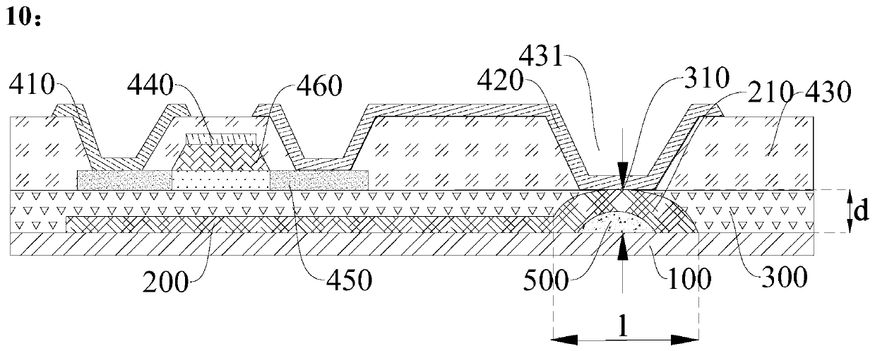
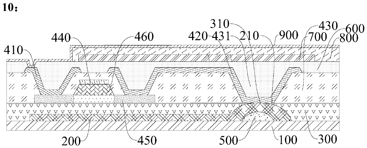
[0025] The present invention is accomplished based on the following findings of the inventors:

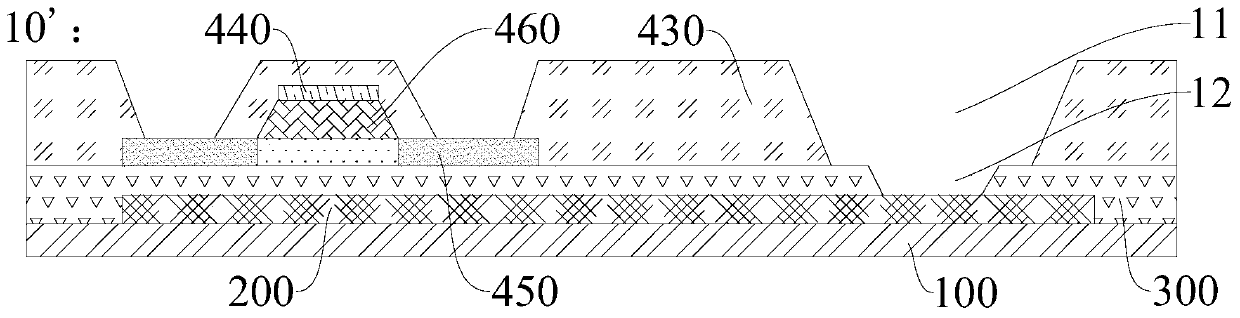
[0026] In related technologies, the inventors have conducted in-depth investigations and a large number of experimental verifications on the reasons why the manufacturing process of the display backplane takes a long time, the production efficiency is low, the display quality of the display device assembled into it is low, and the display effect is not good. , in the manufacturing process of the display backplane of the related art, it is difficult to etch when etching the set holes on the interlayer insulating layer and the buffer layer. Due to the difficulty of the aforementioned etching, the photolithography step requires The time is longer. On the one hand, the photoresist is more likely to be denatured during the longer etching time, so that the photoresist is not easy to be peeled off in the subsequent steps, so that photoresist residue will appear after it is assembled into a...


PUM


Abstract

The invention provides a display backboard, a manufacturing method thereof and a display device. The display backboard comprises a substrate base plate; a shading layer which is arranged on a part ofthe surface of the substrate and is provided with a convex part; a buffer layer which is arranged on the surface of the substrate base plate and the surface, away from the substrate base plate, of theshading layer, wherein an opening is formed in the buffer layer, and at least one part of the protruding part is located in the opening; and a thin film transistor array layer which is arranged on the surfaces, far away from the substrate, of the buffer layer and the convex part; a source electrode and a drain electrode in the thin film transistor array layer are in contact with the protruding part located in the opening through through holes in the interlayer insulating layer, and the distance between the part, away from the underlayer substrate, of the surface of the protruding part locatedin the opening and the underlayer substrate is larger than the distance between the surface, away from the underlayer substrate, of the buffer layer and the underlayer substrate. The display backboard is simple in manufacturing process, easy to produce and not prone to generating poor photoresist residues and poor Mura, and therefore the display device is high in display quality and good in display effect.

Description

technical field [0001] The present invention relates to the field of display technology, in particular, to a display backplane, a manufacturing method thereof, and a display device. Background technique [0002] In the related art, the production process of the display backplane is still time-consuming and the production efficiency is low; in addition, after the display backplane is assembled into a display device, it is more likely to have photoresist residue defects and mura defects, which in turn lead to the failure of the display device. The display quality is lower and the display effect is not good. [0003] Therefore, the related technologies of the existing display backplane still need to be improved. Contents of the invention [0004] The present invention aims to solve one of the technical problems in the related art at least to a certain extent. Therefore, an object of the present invention is to provide a display backplane with simple manufacturing process, e...

Claims


Application Information

Patent Timeline
IPC IPC(8): H01L27/12H01L21/77
CPCH01L27/1218H01L27/1262
Inventor 黄勇潮程磊磊刘军成军王庆贺倪柳松丁远奎周斌闫梁臣
Owner HEFEI XINSHENG OPTOELECTRONICS TECH CO LTD
Why Eureka
Try Eureka