A manufacturing method of an organic light emitting diode display

A technology of light-emitting diodes and manufacturing methods, which is applied in the fields of organic light-emitting devices, organic light-emitting device structures, and semiconductor/solid-state device manufacturing. Effect

Inactive Publication Date: 2019-01-08
WUHAN CHINA STAR OPTOELECTRONICS SEMICON DISPLAY TECH CO LTD
View PDF7 Cites 3 Cited by
  • Summary
  • Abstract
  • Description
  • Claims
  • Application Information

AI Technical Summary

Problems solved by technology

[0002] Because the organic light-emitting polymer in the organic light-emitting diode is easily eroded by oxygen and water, it produces an oxidation reaction, thereby reducing the efficiency and life of the OLED device; in order to prevent the OLED light-emitting layer from being invaded by water and oxygen, prolong the life of the OLED and improve Luminous efficiency. At present, the industry commonly uses a sandwich packaging structure, that is, an inorganic-organic-inorganic packaging structure. In order to ensure strong compactness to block water and oxygen, the surface of the inorganic layer usually does not have good hydrophobicity.
[0003] The current preparation of superhydrophobic films mostly uses perfluorosilane, methyl nonafluorobutyl ether, ethyl perfluorobutyl ether, acetone, etc. as diluents or raw materials, and then uses molecules containing trihydroxysilicon-based active groups as Silicon reagents, silicon-containing reagents such as perfluorodecyltrimethoxysilane, perfluorooctyltrimethoxysilane, octadecyltrimethoxysilane, etc., and then use the sol-gel method to prepare the mixed substrate, and then spray , printing and other methods to prepare it on the surface of the glass substrate, but due to the thick coating thickness of spraying or inkjet printing, the current inkjet printing technology in the industry is controlled between 4 ~ 12um, while the thickness of the packaging inorganic layer is generally only 1um The spraying method cannot guarantee uniformity, and defects such as mura are prone to occur; the superhydrophobic film prepared by this method has a small water drop angle (about 35 degrees), which makes it difficult to attach materials in the bonding process such as polarizers or protective films. achieve an effective fit

Method used


Image

  • A manufacturing method of an organic light emitting diode display
  • A manufacturing method of an organic light emitting diode display
  • A manufacturing method of an organic light emitting diode display

Examples


Embodiment Construction

[0027] The following descriptions of the various embodiments refer to the accompanying drawings to illustrate specific embodiments in which the present invention can be practiced. The directional terms mentioned in the present invention, such as "up", "down", "front", "back", "left", "right", "inside", "outside", "side", etc., are for reference only The orientation of the attached schema. Therefore, the directional terms used are used to illustrate and understand the present invention, but not to limit the present invention. In the figures, structurally similar units are denoted by the same reference numerals.

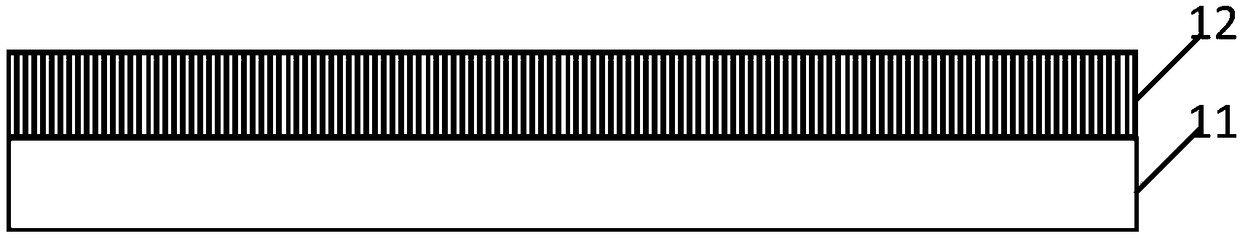
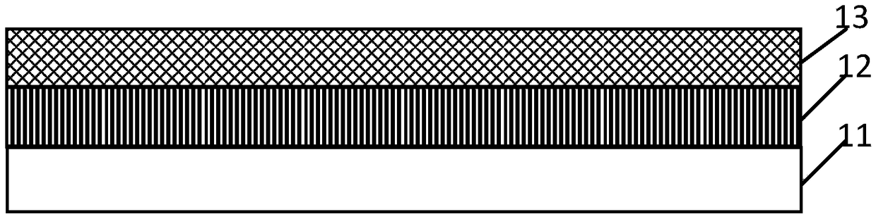
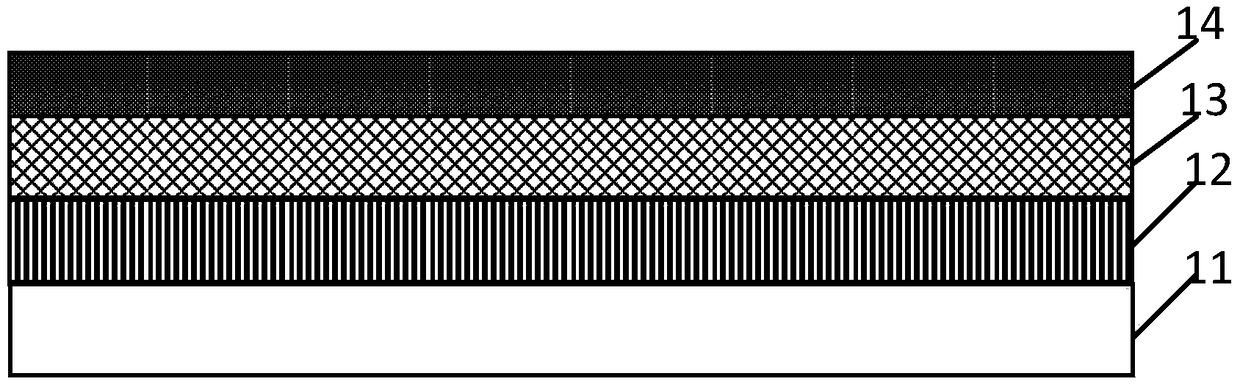
[0028] Please refer to Figures 1 to 4 , figure 1 It is a structural schematic diagram of the first step of the manufacturing method of the organic light emitting diode display of the present invention.

[0029] Such as Figures 1 to 4 As shown, the manufacturing method of the organic light emitting diode display of the present invention mainly includes the follow...


PUM


Abstract

The invention provides a manufacturing method of an organic light emitting diode display. The manufacturing method comprises the following steps: a switch array layer is fabricated on a substrate; Forming an organic light-emitting display layer on the switch array layer; Forming a thin film encapsulation layer on the organic light emitting display layer; A superhydrophobic film is prepare on thatfilm encapsulation layer by a plasma chemical vapor deposition method, and the thickness of the superhydrophobic film is small than a preset thickness. The manufacturing method of the organic light emitting diode display of the invention can improve the uniformity of the film thickness, the density and the surface bonding performance, and the mura is not easy to occur.

Description

【Technical field】 [0001] The invention relates to the field of display technology, in particular to a method for manufacturing an organic light emitting diode display. 【Background technique】 [0002] Because the organic light-emitting polymer in the organic light-emitting diode is easily eroded by oxygen and water, it produces an oxidation reaction, thereby reducing the efficiency and life of the OLED device; in order to prevent the OLED light-emitting layer from being invaded by water and oxygen, prolong the life of the OLED and improve Luminous efficiency, currently the industry commonly uses a sandwich packaging structure, that is, an inorganic-organic-inorganic packaging structure. In order to ensure strong compactness to block water and oxygen, the surface of the inorganic layer usually does not have good hydrophobicity. [0003] The current preparation of superhydrophobic films mostly uses perfluorosilane, methyl nonafluorobutyl ether, ethyl perfluorobutyl ether, aceto...

Claims


Application Information

Patent Timeline
Patent Type & Authority Applications(China)
IPC IPC(8): H01L27/32H01L51/52H01L51/56
CPCH10K59/10H10K50/84H10K71/00H10K50/844H10K71/10H10K50/8445H10K59/1213H10K2102/302
Inventor 王璟朱三
Owner WUHAN CHINA STAR OPTOELECTRONICS SEMICON DISPLAY TECH CO LTD
Why Eureka
Try Eureka