Coset probability based majority-logic decoding for non-binary LDPC codes

a probability-based majority-logic and non-binary ldpc technology, applied in the field of solid-state storage devices, can solve the problems of large performance loss, high error-floor, and affecting the mlgd algorithm for decoding non-binary ldpc codes, and achieve the effect of high error-floor and big performance loss

US20200235753A1Active Publication Date: 2020-07-23NANDEXT SRL
0 Cites 1 Cited by

Patent Information

Authority / Receiving Office
US · United States
Patent Type
Applications(United States)
Current Assignee / Owner
Publication Date
2020-07-23

Smart Images

  • Figure 1
    Figure 1
  • Figure 2
    Figure 2
  • Figure 3
    Figure 3
Patent Text Reader

Abstract

A method for iteratively decoding read bits in a solid state storage device. The read bits are encoded with a Q-ary LDPC code defined over a binary-extension Galois field GF(2r) and having length N. The method comprises determining a binary Tanner graph of the Q-ary LDPC code based on a Q-ary Tanner graph of the Q-ary LDPC code, and based on a binary coset representation of the Galois field GF(2r). The binary Tanner graph comprises, for each Q-ary variable node / Q-ary check node pair of the Q-ary Tanner graph, (2r-1) binary variable nodes each one being associated with a respective one of said cosets; (2r-1-r) binary parity-check nodes each one being connected to one or more of said (2r-1) binary variable nodes according to said binary coset representation of the Galois field GF(2r), wherein each binary parity-check node corresponds to a respective parity-check equation associated with a first parity-check matrix that results from said binary coset representation, and (2r-1) binary check nodes each one being connected to a respective one of said (2r-1) binary variable nodes according to a second parity-check matrix defining the Q-ary LDPC code. The method further comprises, based on a Majority-Logic decoding algorithm, mapping the read bits into N symbols each one including, for each bit thereof, a bit value and a reliability thereof, and providing each symbol of said N symbols to a respective Q-ary variable node, wherein each bit of said each symbol is provided to a respective one of the (2r-1) binary variable nodes of said respective Q-ary variable node. The method also comprises, based on the Majority-Logic decoding algorithm, iteratively performing the following steps: i) at each binary check node, determining a first bit estimate and a first bit reliability of each bit of the respective symbol according to, respectively, a second bit estimate and a second bit reliability of that bit that are determined at each binary variable node connected to that binary check node, and ii) at each binary variable node, updating the second bit estimate and the second bit reliability of each bit of the respective symbol based on the first bit estimate and the first bit reliability of that bit determined at each binary check node connected to that binary variable node, and based on the parity-check equation associated with the first parity-check matrix and corresponding to the parity-check node connected to that binary variable node.
Need to check novelty before this filing date? Find Prior Art

Description

BACKGROUND OF THE INVENTIONField of the Invention

[0001] The present invention generally relates to solid state storage devices, also known as “Solid State Drives” (hereinafter, SSD devices), such as SSD devices provided with non-volatile memory chips (e.g., NAND flash memory chips) for storing data. More particularly, the present invention relates to SSD devices provided with error correction capabilities. Even more particularly, the present invention relates to a SSD device implementing (e.g., in a controller thereof) a method for decoding bits encoded with a non-binary LDPC code.Overview of the Related Art

[0002] SSD devices are nowadays widely used, for example as storage units of computers in replacement of HDD (“Hard Disk Drives”).

[0003] A common SSD device comprises non-volatile memory chips (for example, NAND flash memory chips) each one including non-volatile memory cells for storing data (bits) even in the absence of external power supply, and a SSD device controller (hereinaft...

Examples

Embodiment Construction

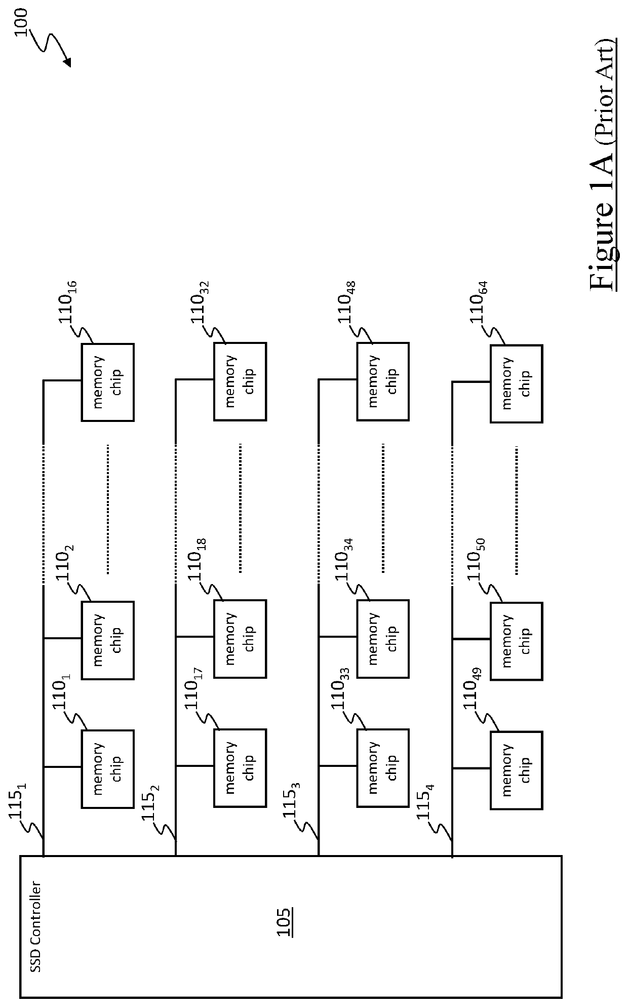
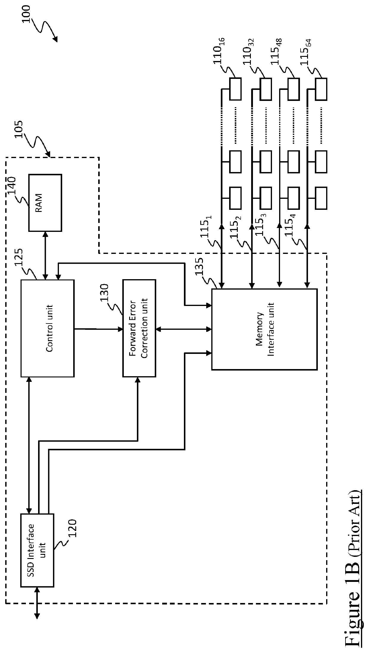
[0072]With reference to the drawings, FIG. 1A schematically shows a simplified architecture of a “Solid State Drive” device (SSD device) 100 known in the state of the art.

[0073]The SSD device 100 preferably comprises a controller (e.g., a processor and / or other control circuitry, referred to herein as SSD controller) 105, a plurality of non-volatile memory chips (e.g. flash memory chips, such as NAND flash memory chips) 110i for storing bits even in the absence of external power supply (i=1, 2, 3, . . . , I, with I=64 in the example at issue), and a plurality of (e.g., synchronous and / or asynchronous) channels 115j (j=1, 2, 3, . . . , J, with J=4 in the example at issue) communicably coupling the SSD controller 105 and the memory chips 110i to each other—in the exemplary illustration, each channel 115j communicably couples the SSD controller 105 to a set of 16 memory chips 110i (e.g., with the channels 1151, 1152, 1153 and 1154 that communicably couple the SSD controller 105 to the ...