
Micro LED transfer method and display module manufactured by the same

Active Publication Date: 2020-11-12
SAMSUNG ELECTRONICS CO LTD
View PDF0 Cites 3 Cited by
  • Summary
  • Abstract
  • Description
  • Claims
  • Application Information

AI Technical Summary

Benefits of technology

The patent is about a display module and a way to make it that puts more micro LEDs on a smaller transfer substrate. The method uses a screen layer to make the laser beam more accurate, which helps to minimize the space between the micro LEDs. The result is a display module that has more micro LEDs in a smaller space.

Problems solved by technology

However, in a case of transferring the micro LEDs in the laser transfer manner, there is a problem that accuracy of the laser beam is non-uniform.
The micro LEDs taking the inclined posture as described above may not be accurately transferred to designated positions on the target substrate resulting in a significant decrease in transfer efficiency.
However, even with such a measure, it was difficult to improve accuracy of a point at which the laser beam is focused on the relay substrate.
For this reason, it was difficult to maximize the number of micro LEDs that may be arranged as compared with an area of the relay substrate.
Due to such a problem, the number of times of replacement of the relay substrate in a transfer process has increased, and a working time required for the transfer process has increased, resulting in an increase in a manufacturing cost.
Also, the disclosure is not required to overcome the disadvantages described above, and an embodiment of the disclosure may not overcome any of the problems described above.

Method used


Image

  • Micro LED transfer method and display module manufactured by the same
  • Micro LED transfer method and display module manufactured by the same
  • Micro LED transfer method and display module manufactured by the same

Examples


Embodiment Construction

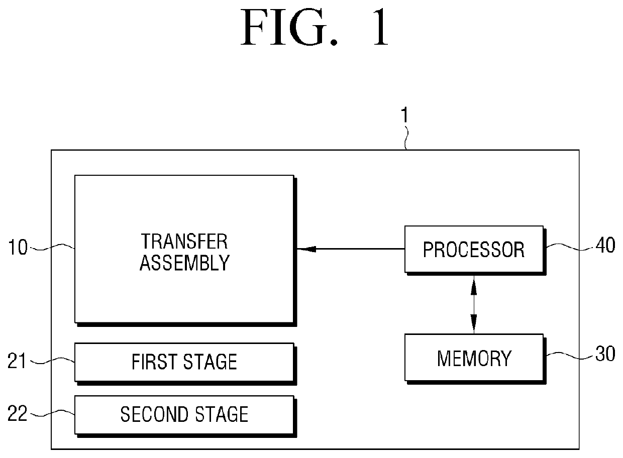
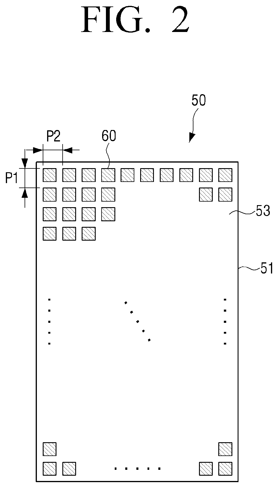
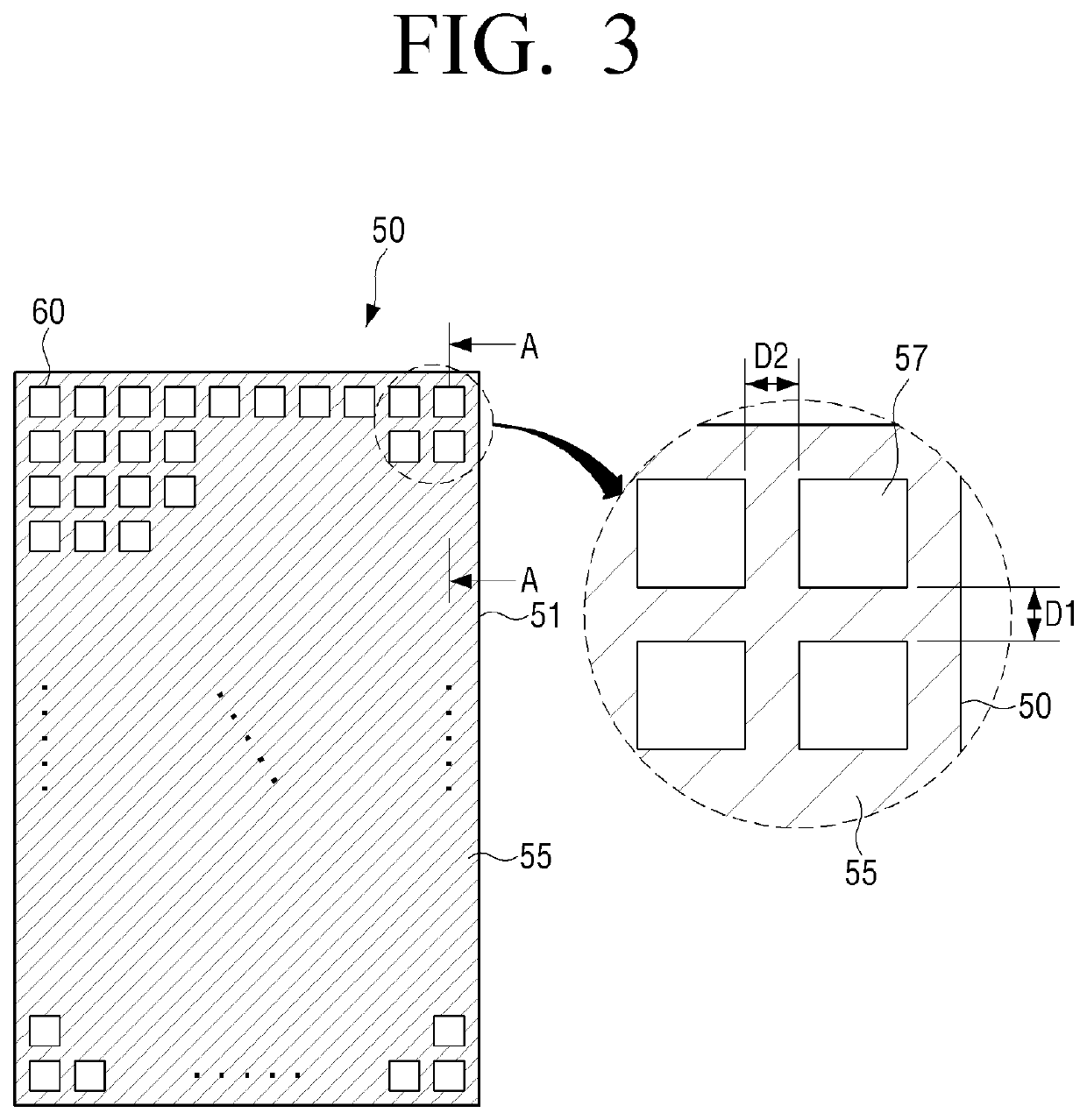
[0034]Embodiments will be described with reference to the accompanying drawings. However, the disclosure is not limited to the embodiments described below, but may be implemented in several forms and may be variously modified. A description for these embodiments is provided only to make the disclosure complete and allow those skilled in the art to which the disclosure pertains to completely recognize the scope of the embodiments. In the accompanying drawings, sizes of components may be enlarged as compared with actual sizes for convenience of explanation, and ratios of the respective components may be exaggerated or reduced.

[0035]It will be understood that when an element is referred to as being “connected,” or “coupled,” to another element, it can be directly connected or coupled to the other element or intervening elements may be present. In contrast, when an element is referred to as being “directly connected,” or “directly coupled,” to another element, there are no intervening e...


PUM


Abstract

A display module is provided. The display module includes: a substrate; a thin film transistor (TFT) layer formed on one surface of the substrate; and a plurality of micro LEDs disposed on the TFT layer. The plurality of micro LEDs are transferred from a transfer substrate to the TFT layer by a laser beam radiated to the transfer substrate through openings of a mask. The openings correspond to regions in which the respective micro LEDs of the transfer substrate are arranged and the openings correspond to a width, a length, or a unit area of each of the micro LEDs.

Description

CROSS-REFERENCE TO RELATED APPLICATION(S)[0001]This application is based on and claims priority under 35 U.S.C. § 119 to Korean Patent Application No. 10-2019-0053285, filed on May 7, 2019, in the Korean Intellectual Property Office, the disclosure of which is incorporated by reference herein in its entirety.BACKGROUNDField[0002]The disclosure relates to a display module and a method of manufacturing the display module by transferring a plurality of LEDs from a micro LED transfer substrate to a target substrate.Description of the Related Art[0003]A plurality of micro light emitting diodes (LEDs) are grown and manufactured in a chip form on a wafer (growth substrate) through an epitaxial process, and the like. The micro LEDs manufactured as described above may be generally transferred onto a relay substrate and then transferred onto a target substrate to configure a display module.[0004]A laser transfer manner may be used to transfer the micro LEDs on the relay substrate to the targe...

Claims


Application Information

Patent Timeline
IPC IPC(8): H01L25/13H01L33/00
CPCH01L33/005H01L25/13H01L33/0095H01L2224/95H01L2224/95001H01L2224/81001H01L2224/81191H01L25/0753H01L25/167H01L33/62H01L27/156H01L27/1214H01L21/67144H01L21/52
Inventor KWAG, DOYOUNGKIM, BYUNGCHULKIM, EUNHYEPARK, SANGMOOOH, MINSUBLEE, DONGYEOBLEE, YOONSUK
Owner SAMSUNG ELECTRONICS CO LTD
Features
  • Generate Ideas
  • Intellectual Property
  • Life Sciences
  • Materials
  • Tech Scout
  • Unparalleled Data Quality
  • Higher Quality Content
  • 60% Fewer Hallucinations
Learn More