Device and method for measuring light energy received by at least one photosite

a technology of light energy and photosites, applied in the field of imaging devices, can solve the problems of reducing the input resistance of the transistor, affecting the sensitivity of the light energy measurement device, so as to achieve the effect of increasing the sensitivity

Inactive Publication Date: 2014-10-21
STMICROELECTRONICS (CROLLES 2) SAS +1
View PDF6 Cites 0 Cited by
  • Summary
  • Abstract
  • Description
  • Claims
  • Application Information

AI Technical Summary

Benefits of technology

[0006]The Staebler-Wronski effect is the origin of the current drift. Specifically, exposing the material encapsulating the transfer transistor to light generates positive charges in the material. The drift of the transistor then results from field-effect depletion of the implanted p-doped surface of the photodiode. This depletion may modify the effective doping of this p-doped region of the photodiode, and therefore, reduces the input resistance of the transistor and leads to modified conduction.
[0009]The more powerful the illumination is and the longer it is applied for, the greater the number of charge carriers generated and the larger the current drift in time may be. Although it is possible to use germanium, the hydrogenated amorphous semiconductor preferably May comprise hydrogenated amorphous silicon. Hydrogenated amorphous silicon may make it possible to maximize the number of dangling bonds and therefore the amount of charge generated under exposure to light, relative to other hydrogenated amorphous semiconductors.
[0011]Although it is possible to use a high proportion of hydrogen, hydrogenated amorphous silicon comprising between 1% and 10% hydrogen (by atomic percentage) may be used. This is because such a percentage range may allow an amorphous structure and therefore a large amount of weak bonds (source of the charge that generates the current drift) to be obtained more easily. The drift of the current in time may therefore be greater.
[0017]The device may also comprise reset-control means or a reset-control module able to apply a potential to the gate of the transfer transistor reversing the direction of the electric field between the gate of the transfer transistor and the photodiode relative to the electric field under nominal operation. Advantageously, the processor may be coupled to the reset module, the reset module being able to control, after the pixel has been reset, measurement of the drain-source current and storage in the memory of the magnitude measured after the reset as a reference magnitude. The device may advantageously comprise a plurality of the pixels coupled in parallel so as to increase its sensitivity.

Problems solved by technology

It has been observed that the material used to encapsulate the transfer transistor causes the current to drift in time.
This depletion may modify the effective doping of this p-doped region of the photodiode, and therefore, reduces the input resistance of the transistor and leads to modified conduction.

Method used


Image

  • Device and method for measuring light energy received by at least one photosite
  • Device and method for measuring light energy received by at least one photosite
  • Device and method for measuring light energy received by at least one photosite

Examples


Embodiment Construction

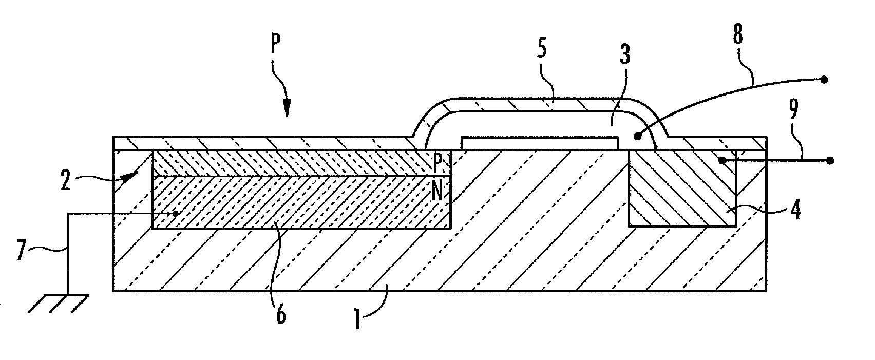
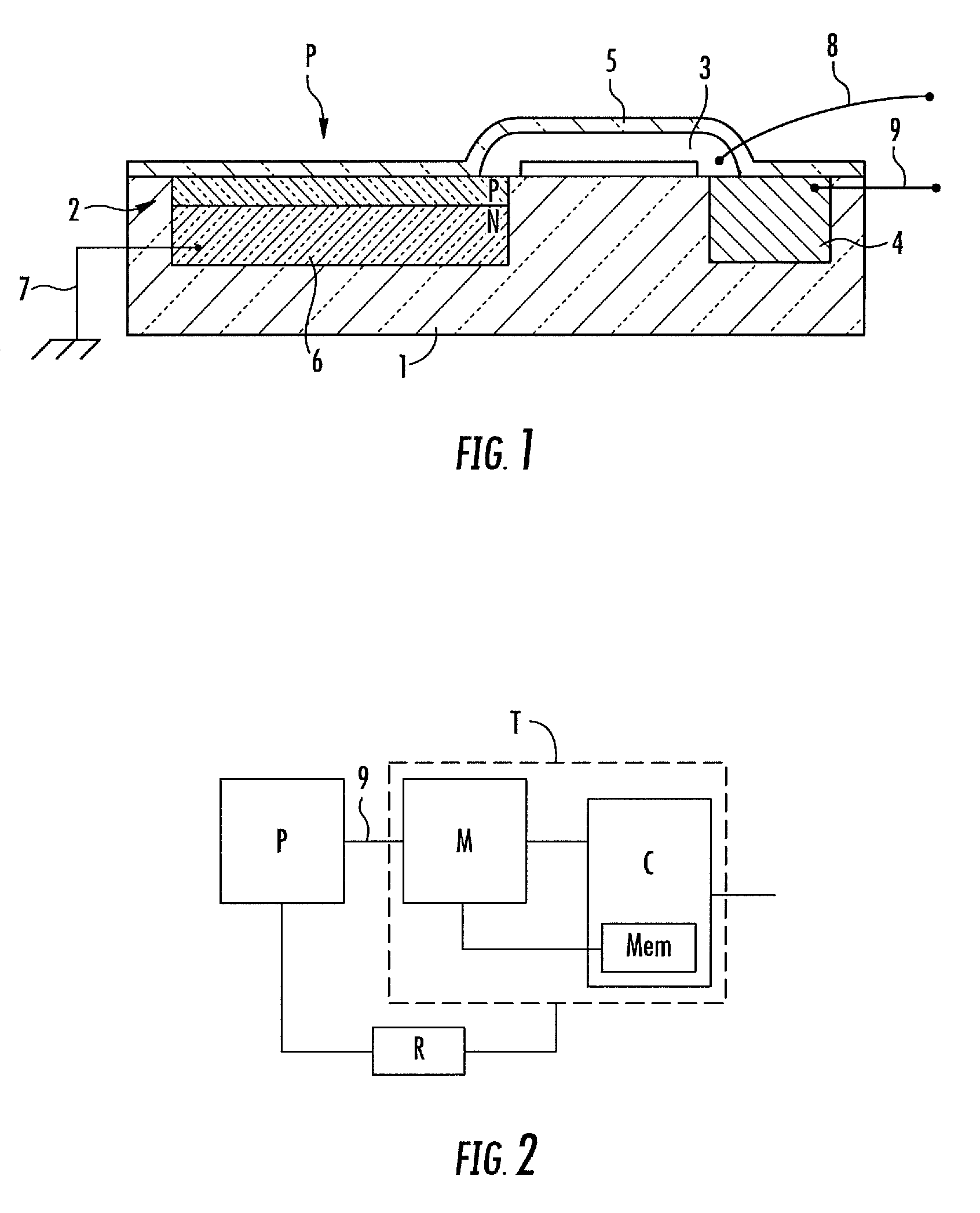
[0022]FIG. 1 shows a pixel P of a device for measuring energy received by the pixel P according to one embodiment. The pixel P formed in a semiconductor substrate 1 comprises a photodiode 2 comprising at least one p-n junction, a transfer transistor 3, and a reading node 4.

[0023]The transfer transistor 3 is coupled on the one hand to the photodiode 2 and on the other hand to the reading node 4. The transfer transistor 3 is encapsulated in a layer 5 of hydrogenated amorphous silicon. This layer 5 of hydrogenated amorphous silicon may cover the entire surface of the pixel P or just part of the gate of the transfer transistor 3.

[0024]The photodiode 2 comprises a charge storage region 6 able to store the charge created via the photoelectric effect in the photodiode. The current created by this charge is removed by grounding the charge storage region 6 via an electrical connection 7, such as a metal contact.

[0025]The gate of the transfer transistor 3 is coupled via an electrical connecti...


PUM


Abstract

A method is for measuring light energy received by a pixel including a transfer transistor, and a photodiode including a charge storage region. The method may include encapsulating the gate of the transfer transistor of the pixel in a semiconductor layer, at least one part of which includes a hydrogenated amorphous semiconductor. The method also may include grounding the charge storage region of the pixel, and determining the drift over time in the magnitude of the drain-source current of the transfer transistor.

Description

FIELD OF THE INVENTION[0001]The invention relates to imaging devices, and more particularly, to a device for measuring light energy received by at least one photosite.BACKGROUND OF THE INVENTION[0002]An imaging device, or sensor, is a photosensitive electronic component used to covert electromagnetic radiation into an analog electrical signal. Generally, this signal is then amplified, digitized by an analog / digital converter, and finally processed so as to obtain a digital image. In this case, the imaging device makes use of the photoelectric effect, whereby incident photons liberate electrons at a semiconductor junction in each active element. To do this, a photosite (e.g. pixel) comprises at least one photosensitive region, for example, a photodiode, and a reading region coupled to the photodiode via a charge transfer transistor.SUMMARY OF THE INVENTION[0003]According to an embodiment, a device having a reduced size is provided for measuring light energy received by at least one p...

Claims


Application Information

Patent Timeline
Patent Type & Authority Patents(United States)
IPC IPC(8): H01L31/0376H01L27/00H01L31/0392H01L31/20H01L27/146
CPCH01L27/14692H01L27/14679H01L27/1462H01L31/202H01L31/03921H01L27/14603H01L31/03767H01L27/14665H01L27/14612Y02P70/50
Inventor BLONKOWSKI, SERGELOPEZ, DIANA
Owner STMICROELECTRONICS (CROLLES 2) SAS
Why Eureka
Try Eureka