
Eureka
For R&D, Eureka makes reading and utilizing patents & technical documents easy.
Eureka AIR
Designed for self-driven R&D workflows. Generate viable solutions, solve complex R&D challenges, empower your innovation with AI.

Eureka Materials
Designed for material experts only. Revolutionize your material R&D, from search, analyze, to developing new materials.

TechResearch
Generate reliable direction feasibility study reports for your R&D in just a few steps.

TechSeek
Discover and master advanced knowledge NOW. Basics, ideas, possibilities, all at once.

TechMind
As an expert in R&D Theories, TechMind can generates customized viable solutions instantly.

TechRisk
Analyze your overall solution with one click, know your potential R&D risks in advance.

TechMonitor
Get weekly tech updates, stay abreast of the latest tech innovations and key insights.
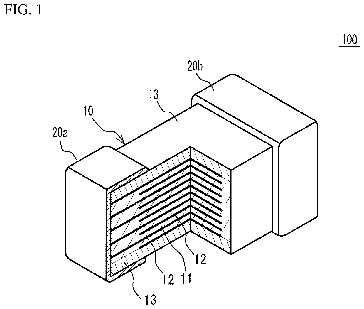
Ceramic electronic device and manufacturing method of the same
- Summary
- Abstract
- Description
- Claims
- Application Information
AI Technical Summary
Benefits of technology
Problems solved by technology
Method used
Image

Examples
examples
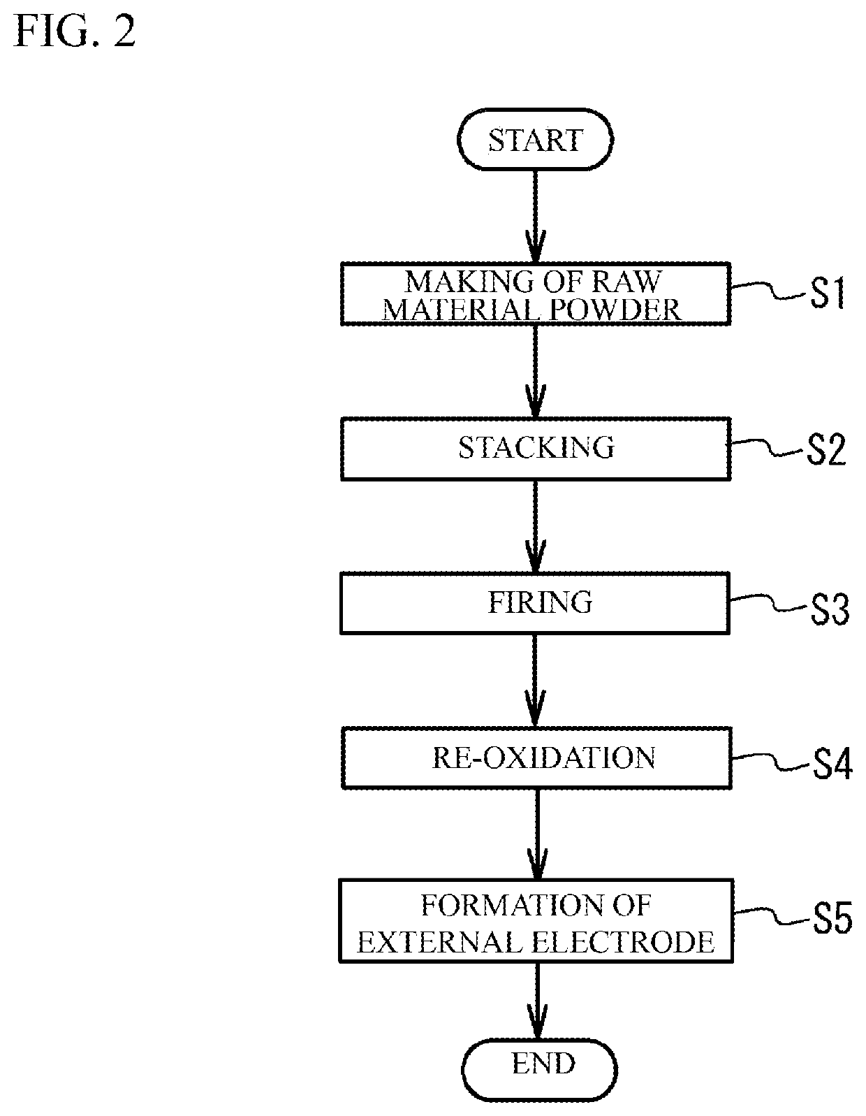
[0051]The multilayer ceramic capacitors in accordance with the embodiment were made and the property was measured.
[0052]BaTiO3 made by a solid-phase reaction method was used as a main component. SiO2, Gd2O3, MgO and MnO were added as sub components. A ratio of Gd2O3 was 0.4 mol, a ratio of SiO2 was 1 mol, a ratio of MgO was 0.45 mol, and a ratio of MnO was 0.1 mol, on a presumption that an amount of BaTiO3 was 100 mol. And, the resulting ceramic powder was sufficiently wet-blended and crushed in a ball mil. Thus, the dielectric material was obtained. An organic binder and a solvent were added to the dielectric material. And dielectric green sheets were made by a doctor blade method. The organic binder was polyvinyl butyral (PVB) resin or the like. The solvent was ethanol, toluene or the like. And a plasticizer and so on were added. Next, the metal conductive paste for forming the internal electrode layers was made by mixing metal powder acting as the main component metal of the inte...
PUM
| Property | Measurement | Unit |
|---|---|---|
| Thickness | aaaaa | aaaaa |
| Substance count | aaaaa | aaaaa |
| Fraction | aaaaa | aaaaa |
Abstract
Description
Claims
Application Information
 - R&D Engineer
- R&D Manager
- IP Professional
- Industry Leading Data Capabilities
- Powerful AI technology
- Patent DNA Extraction
Browse by: Latest US Patents, China's latest patents, Technical Efficacy Thesaurus, Application Domain, Technology Topic, Popular Technical Reports.
© 2024 PatSnap. All rights reserved.Legal|Privacy policy|Modern Slavery Act Transparency Statement|Sitemap|About US| Contact US: help@patsnap.com