

Camera module having chamfer, photosensitive assembly, preparation method, and electronic device
- Summary
- Abstract
- Description
- Claims
- Application Information
AI Technical Summary
Benefits of technology
Problems solved by technology
Method used
Image

Examples
first embodiment
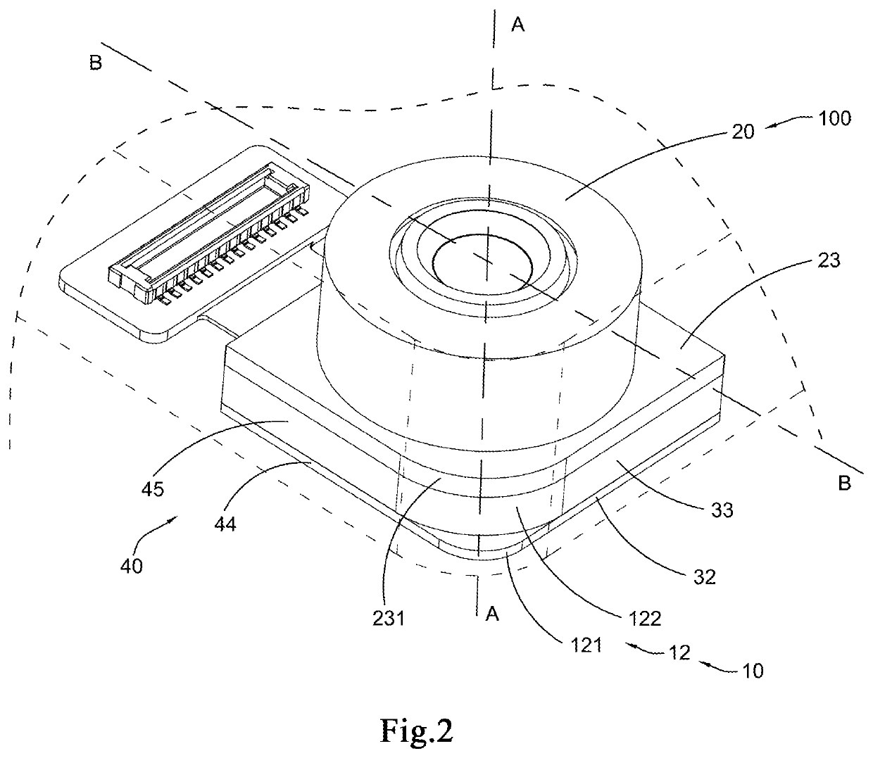
[0124]In the present invention, as shown in FIGS. 2-5, the electronic components 35 are arranged in the side area 42 and / or the corner edge area 43 of the photosensitive assembly 30, so that the photosensitive element 31 may be attached to the circuit board 32 on an upper side, i.e., a width of the top area 41 is narrower relative to other areas (the width is a distance between the edge of the photosensitive chip and the edge of the circuit board). As a result, the optical assembly 20 may be closer to the top side wall of the electronic device, thereby increasing the screen-to-body ratio.
[0125]In the first embodiment of the present invention, the outer edge of the optical lens 21 without chamfer is located at inside of the outer edge of the first chamfer portion 12, so the optical lens 21 may not need additional chamfering process, thereby saving process steps.
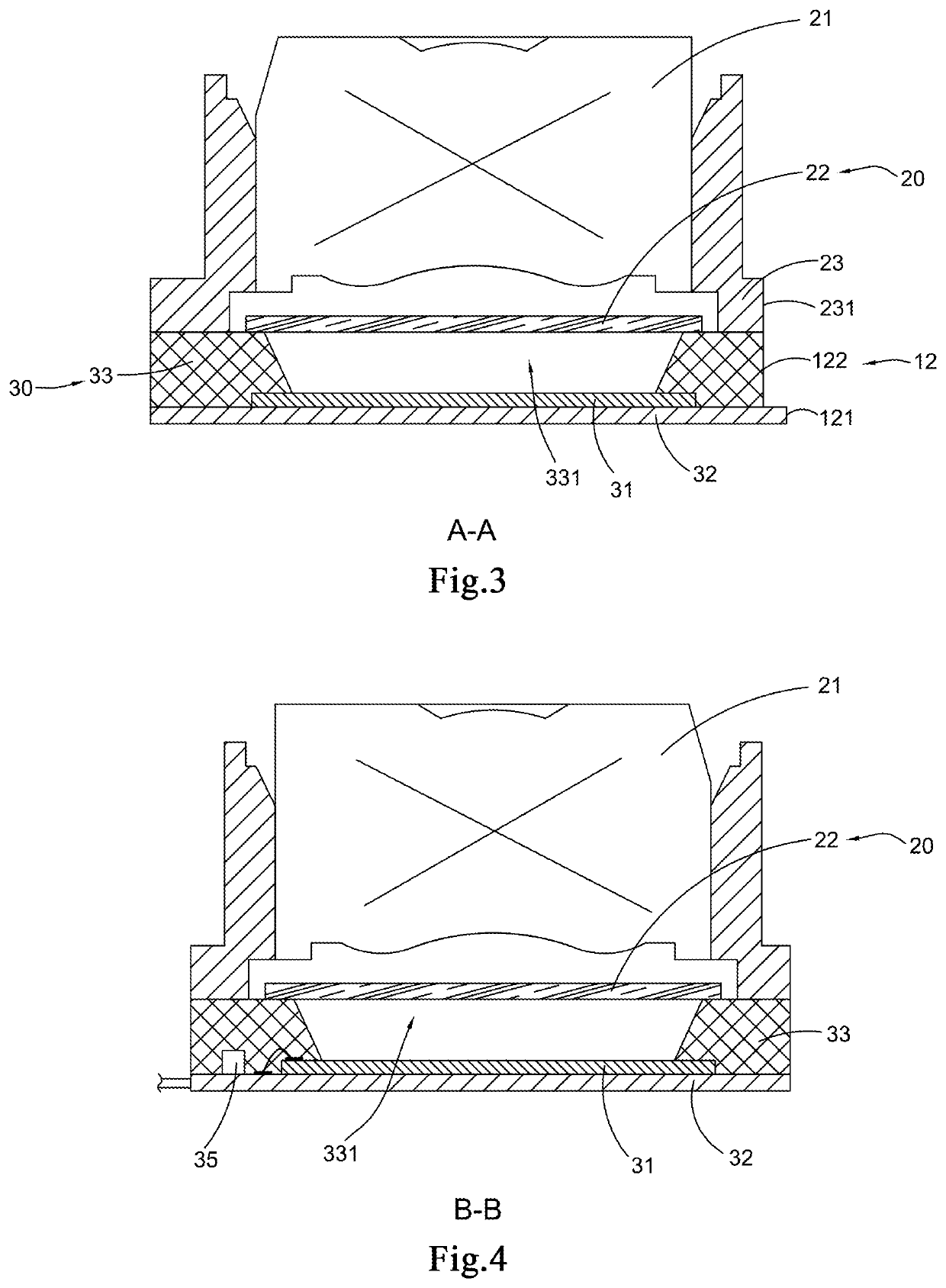
[0126]At this time, the chamfer portion 10 is implemented as the first chamfer portion 12, wherein the first chamfer portion...
second embodiment
[0147]In the present invention, as shown in FIGS. 7-10, a camera module 100A includes an optical assembly 20A and a photosensitive assembly 30A, wherein the photosensitive assembly 30A includes a photosensitive element 31A, a circuit board 32A, a molded body 33A and a series of electronic components 35A, wherein the optical assembly 20A includes an optical lens 21A and a light-transmitting element 22A. The photosensitive assembly 30A has a first chamfer portion 12A and an edge portion 40A, wherein the edge portion 40A has a top area 41A, a side area 42A, and a corner edge area 43A. Correspondingly, the circuit board 32A has a circuit board edge portion 44A and a circuit board chamfer 121A, and the molded body 33A has a molded body chamfer 122A and a molded body edge portion 45A. The optical assembly 20A includes an optical lens 21A and / or a light-transmitting element 22A, and the optical lens 21A may be further installed at the photosensitive assembly 30A through an installation sur...
PUM
 Abstract
Description
Claims
Application Information