Multiplication and accumulation (MAC) operator
- Summary
- Abstract
- Description
- Claims
- Application Information
AI Technical Summary
Benefits of technology
Problems solved by technology
Method used
Image

Examples
first embodiment
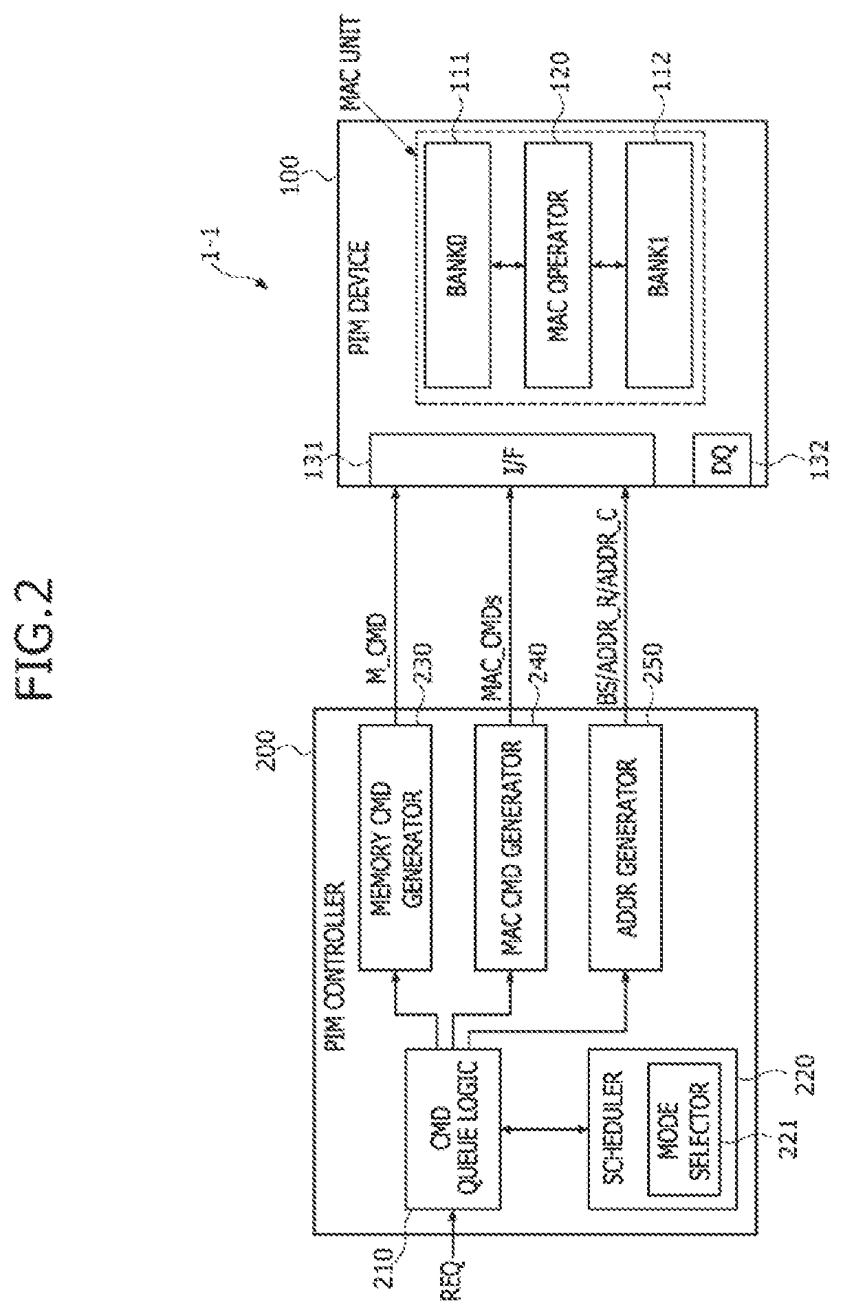
[0083]FIG. 2 is a block diagram illustrating a PIM system 1-1 according to the present disclosure. As illustrated in FIG. 2, the PIM system 1-1 may include a PIM device 100 and a PIM controller 200. The PIM device 100 may include a first memory bank (BANK0) 111, a second memory bank (BANK1) 112, a MAC operator 120, an interface (I / F) 131, and a data input / output (I / O) pad 132. For an embodiment, the MAC operator 120 represents a MAC operator circuit. The first memory bank (BANK0) 111, the second memory bank (BANK1) 112, and the MAC operator 120 included in the PIM device 100 may constitute one MAC unit. In another embodiment, the PIM device 100 may include a plurality of MAC units. The first memory bank (BANK0) 111 and the second memory bank (BANK1) 112 may represent a memory region for storing data, for example, a DRAM device. Each of the first memory bank (BANK0) 111 and the second memory bank (BANK1) 112 may be a component unit which is independently activated and may be configur...
second embodiment
[0141]FIG. 20 is a block diagram illustrating a PIM system 1-2 according to the present disclosure. In FIG. 20, the same reference numerals or the same reference symbols as used in FIG. 2 denote the same elements. As illustrated in FIG. 20, the PIM system 1-2 may be configured to include a PIM device 400 and a PIM controller 500. The PIM device 400 may be configured to include a memory bank (BANK) 411 corresponding to a storage region, a global buffer 412, a MAC operator 420, an interface (I / F) 431, and a data input / output (I / O) pad 432. For an embodiment, the MAC operator 420 represents a MAC operator circuit. The memory bank (BANK) 411 and the MAC operator 420 included in the PIM device 400 may constitute one MAC unit. In another embodiment, the PIM device 400 may include a plurality of MAC units. The memory bank (BANK) 411 may represent a memory region for storing data, for example, a DRAM device. The global buffer 412 may also represent a memory region for storing data, for exam...
third embodiment
[0188]FIG. 29 is a block diagram illustrating a PIM system 1-3 according to the present disclosure. As illustrated in FIG. 29, the PIM system 1-3 may have substantially the same configuration as the PIM system 1-1 illustrated in FIG. 2 except that a PIM controller 200A of the PIM system 1-3 further includes a mode register set (MRS) 260 as compared with the PIM controller 200 of the PIM system 1-1. Thus, the same explanation as described with reference to FIG. 2 will be omitted hereinafter. The mode register set 260 in the PIM controller 200A may receive an MRS signal instructing arrangement of various signals necessary for the MAC arithmetic operation of the PIM system 1-3. In an embodiment, the mode register set 260 may receive the MRS signal from the mode selector 221 included in the scheduler 220. However, in another embodiment, the MRS signal may be provided by an extra logic circuit other than the mode selector 221. The mode register set 260 receiving the MRS signal may transm...
PUM
 Abstract
Description
Claims
Application Information
 - Generate Ideas
- Intellectual Property
- Life Sciences
- Materials
- Tech Scout
- Unparalleled Data Quality
- Higher Quality Content
- 60% Fewer Hallucinations
Browse by: Latest US Patents, China's latest patents, Technical Efficacy Thesaurus, Application Domain, Technology Topic, Popular Technical Reports.
© 2025 PatSnap. All rights reserved.Legal|Privacy policy|Modern Slavery Act Transparency Statement|Sitemap|About US| Contact US: help@patsnap.com