
Three dimensional double-density memory array

a memory array and double-density technology, applied in the field of semiconductor devices, can solve the problems of unstable word line patterns, large number of word lines that require more decoders, and high word line resistance, and achieve the effect of less word lines, less word line decoders, and less word lines

Pending Publication Date: 2021-09-23
HSU FU CHANG
View PDF0 Cites 4 Cited by
  • Summary
  • Abstract
  • Description
  • Claims
  • Application Information

AI Technical Summary

Benefits of technology

This patent describes methods and equipment for making double-density three-dimensional (3D) arrays of memory devices. These arrays can be used in various types of memory technologies, such as NAND flash memory, RRAM, PCM, FRAM, MRAM, etc. The arrays have strings of memory devices, where a portion of the devices form a first channel and another portion of the devices form a second channel. The array also has one set of word lines that connect with devices in both channels. This design reduces the number of word lines, which leads to lower resistance and fewer decoders. It also improves the manufacturing process yield, resulting in better quality memory devices.

Problems solved by technology

However, having many word line connections results is several disadvantages.
For example, there is high word line resistance, and the large number of word lines requires more decoders.
Furthermore, during manufacture, conventional arrays may have low process yields and result in unstable word line patterns.

Method used


Image

  • Three dimensional double-density memory array
  • Three dimensional double-density memory array
  • Three dimensional double-density memory array

Examples


Embodiment Construction

[0039]In various exemplary embodiment, methods and apparatus are provided for the design, construction, and operation of double-density 3D memory arrays.

[0040]Those of ordinary skilled in the art will realize that the following detailed description is illustrative only and is not intended to be in any way limiting. Other embodiments of the present invention will readily suggest themselves to such skilled persons having the benefit of this disclosure. Reference will now be made in detail to implementations of the exemplary embodiments of the present invention as illustrated in the accompanying drawings. The same reference indicators (or numbers) will be used throughout the drawings and the following detailed description to refer to the same or like parts.

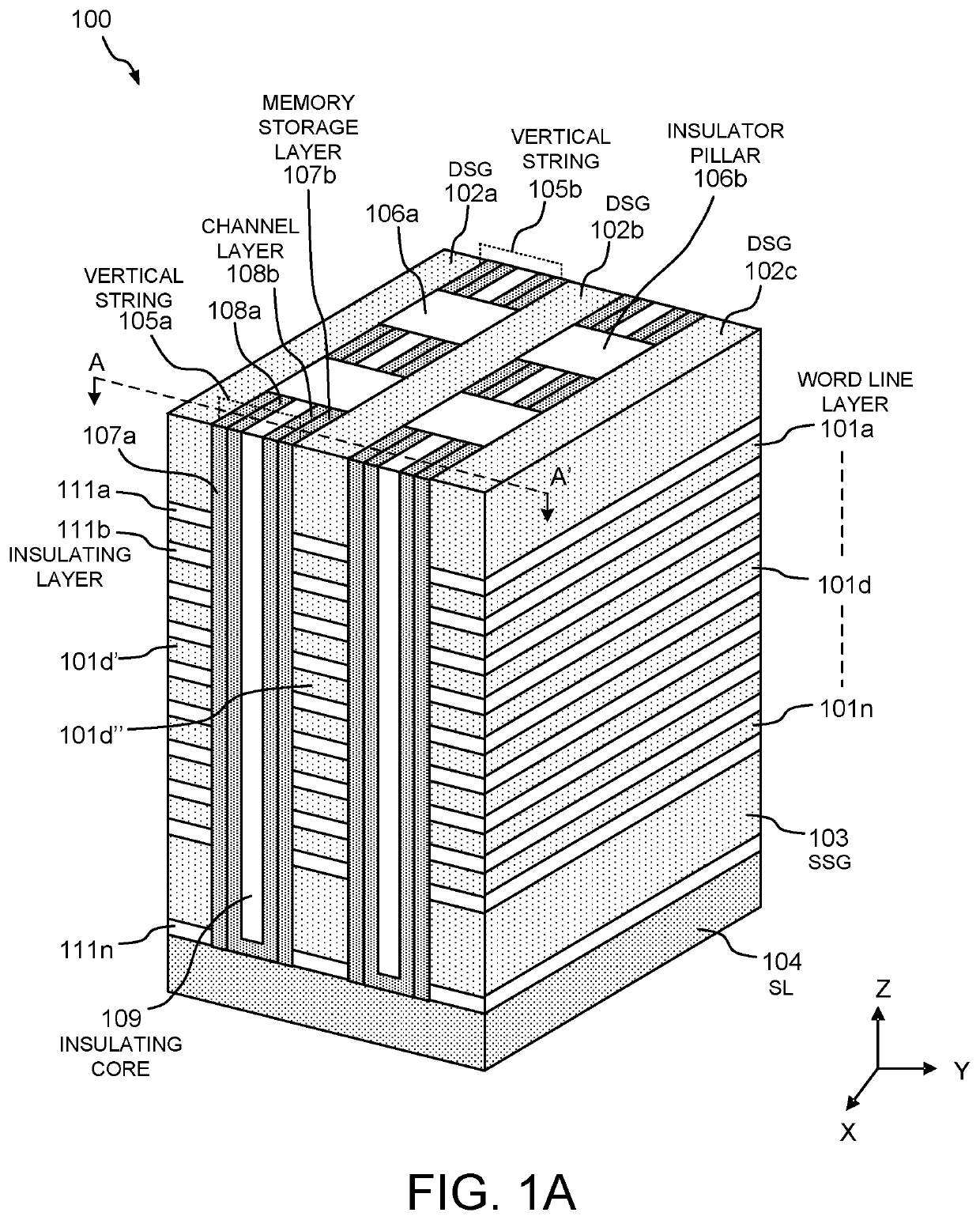
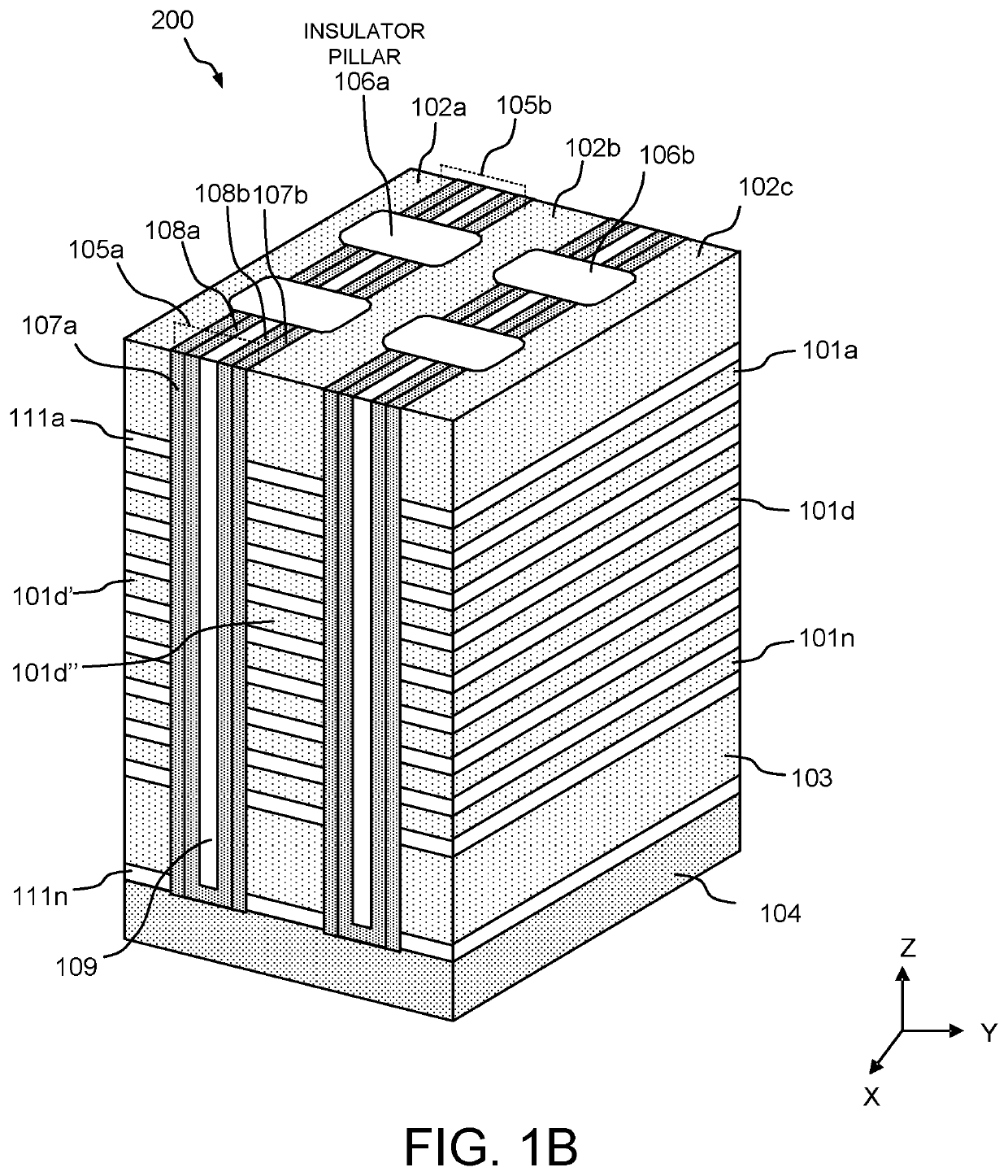
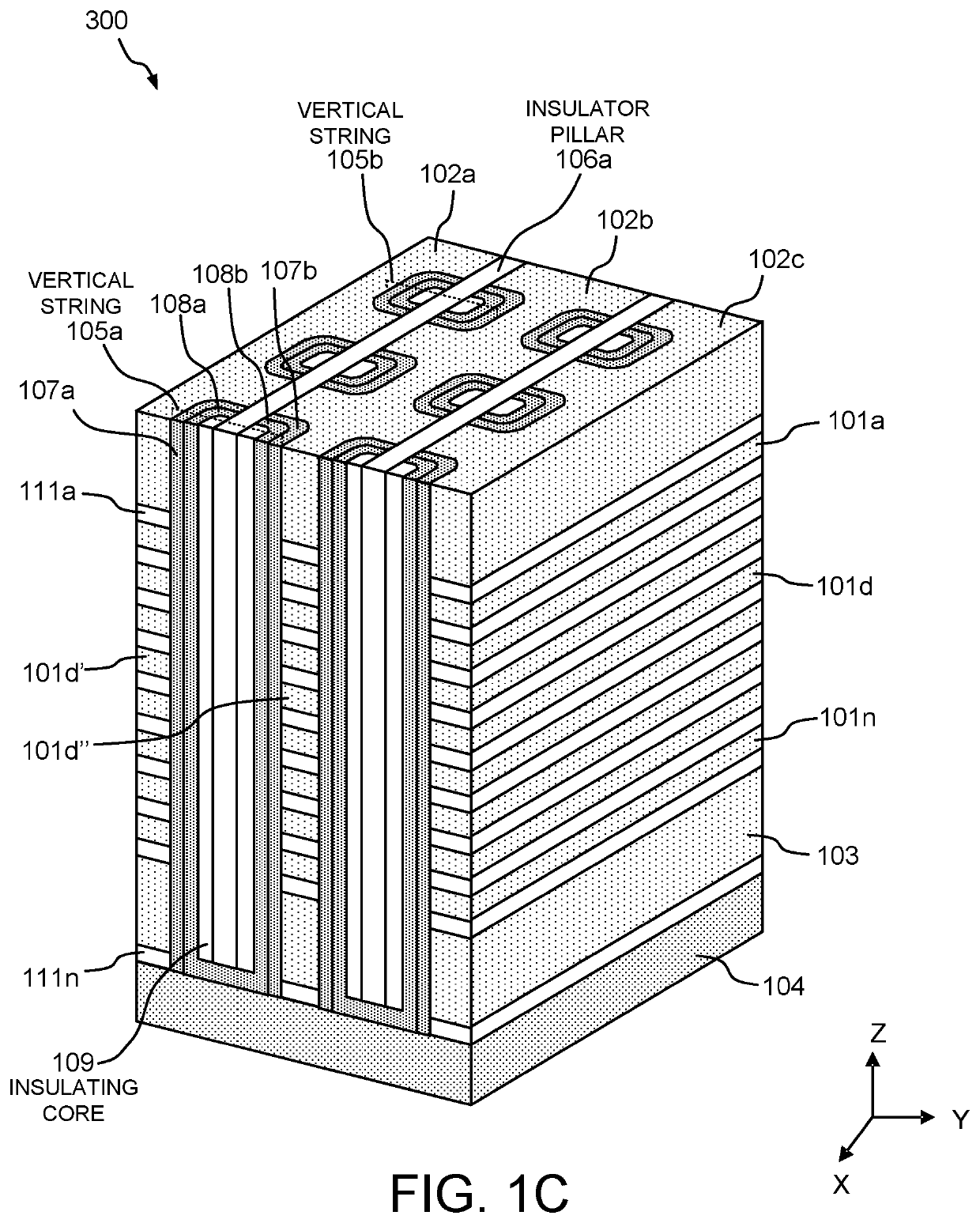
[0041]FIG. 1A shows an exemplary embodiment of a double-density 3D NAND flash memory array 100 constructed in accordance with the invention. The array 100 comprises multiple word line layers, such as word line layers 101a-n. The arra...


PUM


Abstract

A three dimensional double-density memory array is disclosed. In an embodiment, a three-dimensional (3D) double density array comprises a string of memory devices that are configured so that a first portion of the memory devices form a first channel and a second portion of the memory devices form a second channel. The array also comprises a plurality of word lines coupled to the string of memory devices. Each word line is coupled to a memory device that forms the first channel and a memory device that forms the second channel. The array also comprises at least one drain select gate that couples the first and second channels to a bit line.

Description

CROSS-REFERENCE TO RELATED APPLICATIONS[0001]This application claims the benefit under 35 U.S.C. § 119 of U.S. Provisional Patent Application No. 62 / 992,985 filed on Mar. 21, 2020 and entitled “3D MEMORY ARRAY STRUCTURE,” which is incorporated by reference herein in its entirety.FIELD OF THE INVENTION[0002]The exemplary embodiments of the present invention relate generally to the field of semiconductors and integrated circuits, and more specifically to the design, construction, and operation of three dimensional double-density arrays.BACKGROUND OF THE INVENTION[0003]A conventional double-density three dimensional (3D) array includes pairs of vertical strings and each string is connected to its own set of word lines. Typically, even word lines are connected to one vertical string, and odd word line are connected to the another vertical string. However, having many word line connections results is several disadvantages. For example, there is high word line resistance, and the large nu...

Claims


Application Information

Patent Timeline
Patent Type & Authority Applications(United States)
IPC IPC(8): H01L27/11582H01L27/24H01L27/22H01L27/11597H01L27/112G11C11/16G11C11/22G11C13/00G11C16/10G11C16/26G11C17/18
CPCH01L27/11582G11C2213/75H01L27/249H01L27/228H01L27/11597H01L27/11206G11C11/1675G11C11/1673G11C11/2275G11C11/2273G11C13/0069G11C13/004G11C16/10G11C16/26G11C17/18G11C2213/71H01L27/2454G11C16/08G11C16/0483G11C16/24G11C13/0023G11C13/0026G11C13/0028G11C13/003G11C2213/72G11C2213/77G11C13/0002G11C11/1655G11C11/1657G11C11/2255G11C11/2257H10B63/34H10B63/845H10N70/231H10N70/24H10N70/823H10N70/8833H10B43/10H10B43/27H10B51/10H10B51/20G11C11/56H10B20/25H10B20/20H10B61/22
Inventor HSU, FU-CHANG
Owner HSU FU CHANG
Learn More