Memory device with reduced word line resistance

a memory device and word line resistance technology, applied in the field of memory devices, can solve the problems of large number of word line drivers occupying disadvantageously a large layout area, erroneous read/write operation of accessed memory cells, etc., and achieve the effect of reducing the word line resistance and minimizing the layout area

Active Publication Date: 2005-12-08
SAMSUNG ELECTRONICS CO LTD
View PDF6 Cites 37 Cited by
  • Summary
  • Abstract
  • Description
  • Claims
  • Application Information

AI Technical Summary

Benefits of technology

[0018] Accordingly, a memory device is formed with reduced word line resistance and minimized layout area.

Problems solved by technology

Such reduced current may result in an erroneous read / write operation for the accessed memory cell 10.
Such a large number of word line drivers disadvantageously occupy a large layout area.

Method used


Image

  • Memory device with reduced word line resistance
  • Memory device with reduced word line resistance
  • Memory device with reduced word line resistance

Examples


Embodiment Construction

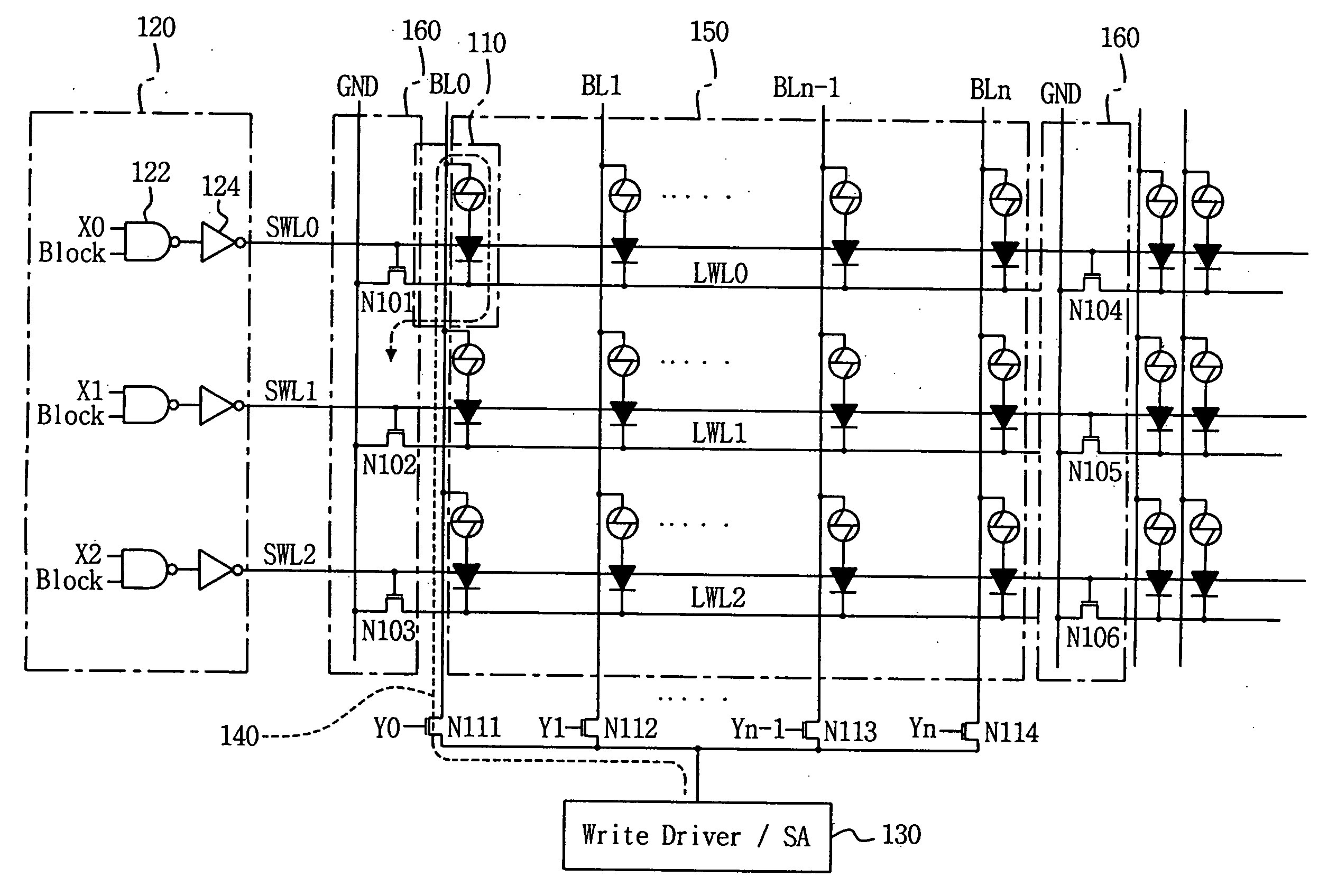
[0031]FIG. 3 is a block diagram of a semiconductor memory device according to an embodiment of the present invention. The semiconductor memory device of FIG. 3 includes a global word line driver 120, local word line drivers 160, and memory blocks 150.

[0032] The local word line drivers 160 are controlled by a global word line driver 120. Each memory block 150 is coupled to a respective local word line driver 160. Each memory block 150 is comprised of a sub-array of memory cells. The local word line drivers 160 and the memory blocks 150 form a main array 200 of memory cells for the semiconductor memory device of FIG. 3.

[0033]FIG. 4 shows a circuit diagram of elements of the semiconductor memory device of FIG. 3, including an example memory block 150 and examples local word line drivers 160, and the global word line driver 120. Referring to FIG. 4, the memory block 150 includes an array of memory cells 110 arranged in rows and columns.

[0034] In addition, the memory block 150 also in...


PUM


Abstract

A memory device includes a plurality of blocks, with each block having a respective array of memory cells and respective local word lines. The memory device also includes a respective switching device coupled between each local word line and a common voltage node. A global word line driver controls the respective switching devices to turn on for respective local word lines in a row across the blocks including an accessed memory cell. Thus, the common voltage node is in the current path of the accessed memory cell with minimized layout area and resistance of the current path.

Description

BACKGROUND OF THE INVENTION [0001] This application claims priority to Korean Patent Application No. 2004-41678, filed on Jun. 8, 2004, in the Korean Intellectual Property Office, the disclosure of which is hereby incorporated by reference in its entirety. [0002] 1. Field of the Invention [0003] The present invention relates generally to memory devices, and more particularly to reducing resistance of a word line in a current path of an accessed memory cell. [0004] 2. Description of the Related Art [0005] A PRAM (Phase-change Random Access Memory) device is being developed as one of the next-generation memory devices for higher performance and lower power consumption. A PRAM device is a nonvolatile memory device for storing data by using a phase change material such as GexSbyTez (hereinafter referred to as ‘GST’). [0006] The resistance of the phase change material is controlled by changing the state of the phase change material to be amorphous or crystalline. Such a state may be cont...

Claims


Application Information

Patent Timeline
Patent Type & Authority Applications(United States)
IPC IPC(8): G11C13/00G11C8/00G11C8/08G11C8/14G11C13/02
CPCG11C8/08G11C8/14G11C13/0004G11C13/0028G11C5/063
Inventor CHO, BEAK-HYUNGKIM, DU-EUNG
Owner SAMSUNG ELECTRONICS CO LTD
Why Eureka
Try Eureka