Method of forming a gate of a flash memory device

a technology of flash memory and gate, which is applied in the direction of semiconductor devices, basic electric elements, electrical equipment, etc., can solve the problems of non-uniform thickness of oxide layer , non-uniform oxide layer , so as to reduce the resistance of the word line and enhance the operation speed of the flash memory device

Inactive Publication Date: 2006-07-20
DONGBU HITEK CO LTD
View PDF10 Cites 5 Cited by
  • Summary
  • Abstract
  • Description
  • Claims
  • Application Information

AI Technical Summary

Benefits of technology

[0024] According to an exemplary embodiment of the present invention, the operation speed of the flash memory device may be enhanced by reducing resistance of the word line.

Problems solved by technology

However, such an oxide layer may be non-uniformly formed due to plasma used in the common-source etching.
However, the oxide layer 27 may be non-uniformly formed due to plasma used in the common source etching.
Such a non-uniform thickness of the oxide layer 27 may induce several problems.
For example, resistance of the gate 20 may be undesirably increased due to the non-uniform thickness of the oxide layer 27.
Therefore, an undesired increase of the resistance of the gate 20 may induce the characteristic degradation of a flash memory device.

Method used


Image

  • Method of forming a gate of a flash memory device
  • Method of forming a gate of a flash memory device
  • Method of forming a gate of a flash memory device

Examples


Embodiment Construction

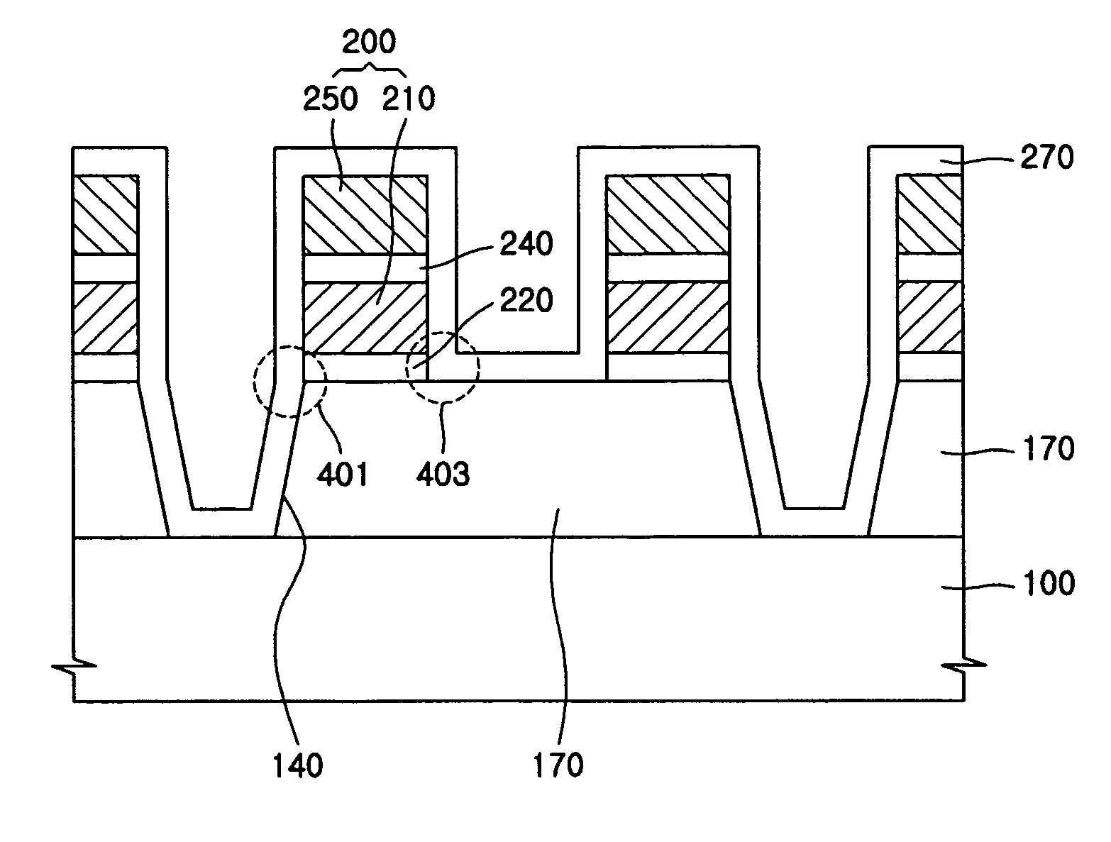
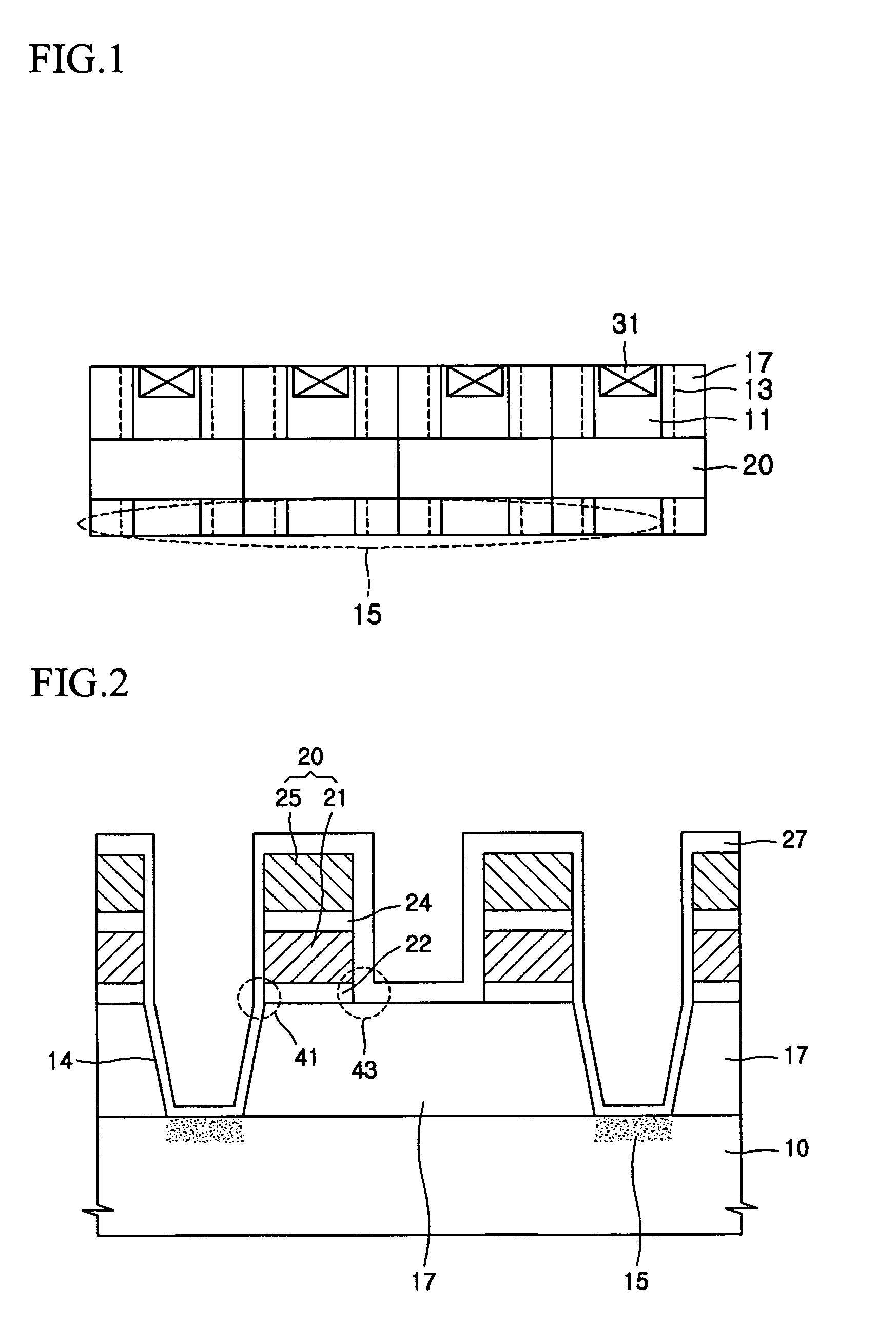
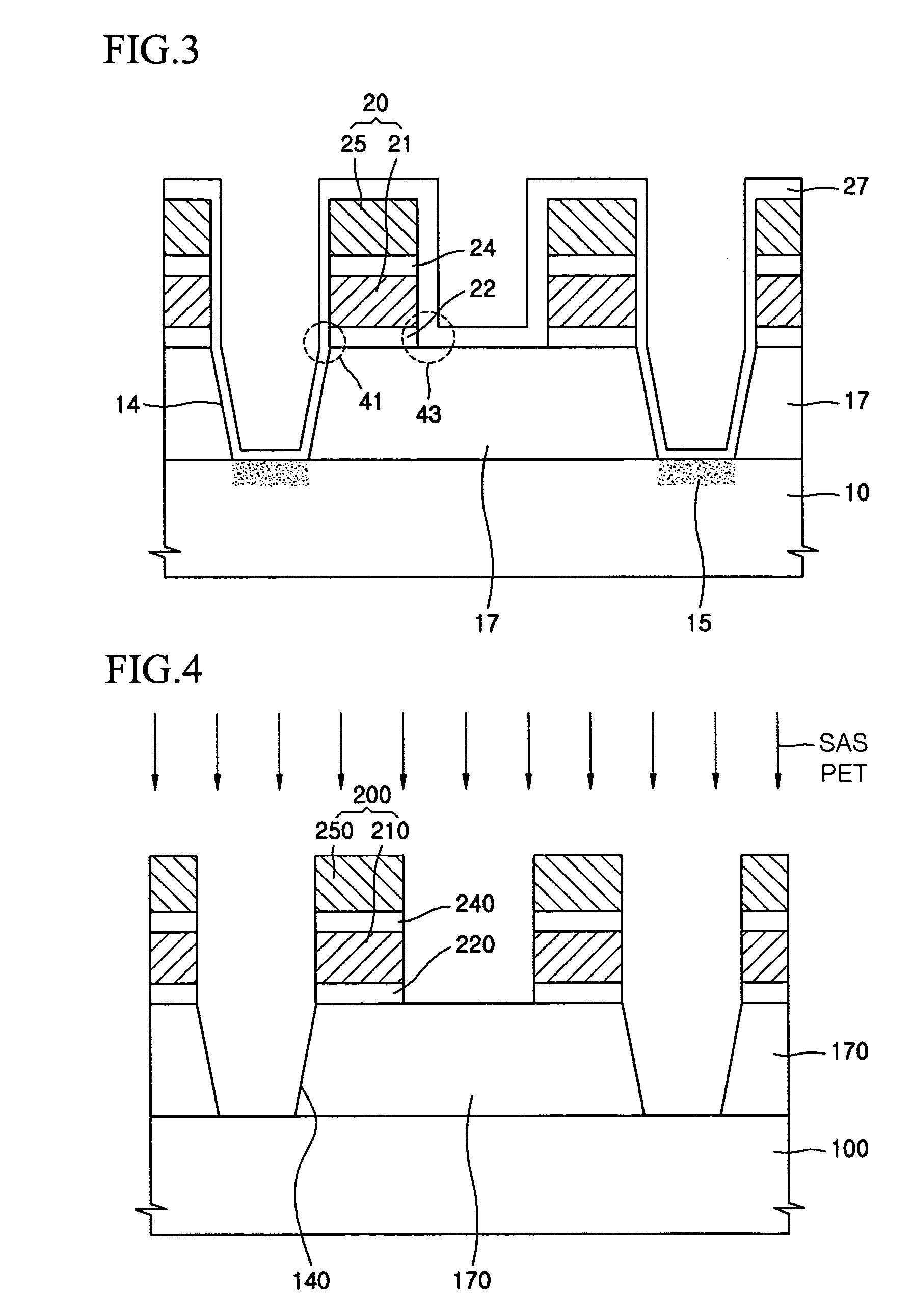
[0028] With reference to the accompanying drawings, the present invention will be described in order for those skilled in the art to be able to implement the invention. As those skilled in the art would realize, the described embodiments may be modified in various different ways, all without departing from the spirit or scope of the present invention.

[0029] To clarify multiple layers and regions, the thicknesses of the layers are enlarged in the drawings. Like reference numerals designate like elements throughout the specification. When it is said that any part, such as a layer, film, area, or plate is positioned on another part, it means the part is directly on the other part or above the other part with at least one intermediate part. On the other hand, if any part is said to be positioned directly on another part it means that there is no intermediate part between the two parts.

[0030] According to an exemplary embodiment of the present invention, in order to enhance operation c...


PUM


Abstract

The present invention provides a method of forming a gate in a flash memory device. The method includes: forming a oxide layer on a semiconductor substrate; forming a stacked structure including a tunnel oxide layer, a floating gate, a dielectric layer, and a control gate by patterning them on the semiconductor substrate; exposing portions of the semiconductor substrate below the field oxide layer by selectively etching the field oxide layer adjacent to the source region in order to form a common source; performing subsequent etching for removing oxides between the control gates; and forming an oxide layer covering the semiconductor substrate and both sidewalls of the floating gate and control gate.

Description

CROSS-REFERENCE TO RELATED APPLICATION [0001] This application claims priority to and the benefit of Korean Patent Application No. 10-2004-0117151 filed in the Korean Intellectual Property Office on Dec. 30, 2004, the entire contents of which are incorporated herein by reference. BACKGROUND OF THE INVENTION [0002] (a) Field of the Invention [0003] The present invention relates to a method of forming a gate in a flash memory device, and more particularly, to a method of forming a gate in a flash memory device having advantages of enhancing an operation speed of a device by reducing resistance of a word line. [0004] (b) Description of the Related Art [0005] A NOR type of flash memory device is a non-volatile memory device having a floating gate and a control gate in its stacked structure. A stacked structure including a floating gate and a control gate is formed in a dual conductive polysilicon structure. The stacked structure is formed on a tunnel oxide layer. An ONO (Oxide—Nitride—O...

Claims


Application Information

Patent Timeline
Patent Type & Authority Applications(United States)
IPC IPC(8): H01L21/336
CPCH01L27/115H01L27/11521H10B69/00H10B41/30H01L21/30604
Inventor KIM, DONG-OOG
Owner DONGBU HITEK CO LTD
Why Eureka
Try Eureka