Substrate processing method and substrate processing apparatus

a substrate processing and substrate technology, applied in the direction of photomechanical treatment, instruments, electric discharge tubes, etc., can solve the problems of reducing the consumption of spm, difficult to reuse spm, and substrates with high energy damage, so as to eliminate suppress the formation of wrinkles in the ink discharge range. , the effect of reducing the need for spm

Pending Publication Date: 2021-09-30
DAINIPPON SCREEN MTG CO LTD
View PDF5 Cites 0 Cited by
  • Summary
  • Abstract
  • Description
  • Claims
  • Application Information

AI Technical Summary

Benefits of technology

[0004]In plasma ashing, carbon bonds of the resist film can be efficiently broken by the collision of the active species mainly including cations with the resist film. On the other hand, there is a problem that cations having a high energy damage is the substrate.
[0008]In the invention (substrate processing method) thus configured, the radical supply step of supplying the radicals to the resist film and the resist removal step of removing the resist film from the front surface of the substrate by supplying the organic solvent having the low surface tension to the resist film on the front surface of the substrate after the radical supply step are performed. When a plasma is generated under an atmospheric pressure, most of ionic molecules, out of active species produced react with molecules in the atmosphere and disappear in a moment. Out of the remaining active species, electrically neutral free radicals are supplied to the resist film. Most of the ionic molecules, which are a main cause to damage the substrate, are not supplied to the resist film. Further, when the radical supply step is finished, the resist film is present on the front surface of the substrate and not removed yet. Thus, damage on the substrate is suppressed. The radicals having reached the front surface of the resist film penetrate into the front surface of the resist film to deteriorate the vicinity of the front surface of the resist film. As a result, fine cracks and holes are formed near the front surface of the resist film. Subsequently, when the organic solvent is supplied, the organic solvent penetrates into these cracks and holes to expand these cracks and holes. In this way, a chemical action, i.e. deterioration by the active species and a physical action, i.e. expansion of the holes and cracks by the organic solvent having the low surface tension are coupled, and the removal of the resist film is accomplished. In this way, it is possible to suppress damage on the substrate in removing the resist film using a plasma and eliminate need for the use of SPM.
[0010]According to the inventor's research, the deterioration of a front surface of a resist film on a substrate under an atmospheric pressure is thought to be largely affected by the action of hydroxyl radicals. Accordingly, in the substrate processing apparatus according to the invention, the distance from the electrode in the active species nozzle to the resist film on the substrate held by the holder is set at such a distance that the hydroxyl radicals included in the active species reach the front surface of the resist film from the electrode within the lives of the hydroxyl radicals. In this way, the front surface of the resist film can be efficiently deteriorated.
[0011]As described above, according to the invention, it is possible to suppress damage on a substrate and eliminate need for the use of SPM in removing a resist film using a plasma.
[0012]As described above, according to the invention, the formation of wrinkles in an ink discharge range can be suppressed in printing an image by discharging ink to a printing medium while conveying the printing medium in a conveying direction.

Problems solved by technology

On the other hand, there is a problem that cations having a high energy damage is the substrate.
The reuse of the SPM is difficult and it has been a problem in recent years to decrease the consumption of the SPM.

Method used


Image

  • Substrate processing method and substrate processing apparatus
  • Substrate processing method and substrate processing apparatus
  • Substrate processing method and substrate processing apparatus

Examples


Embodiment Construction

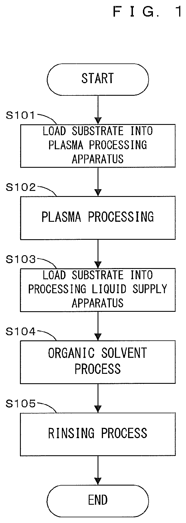
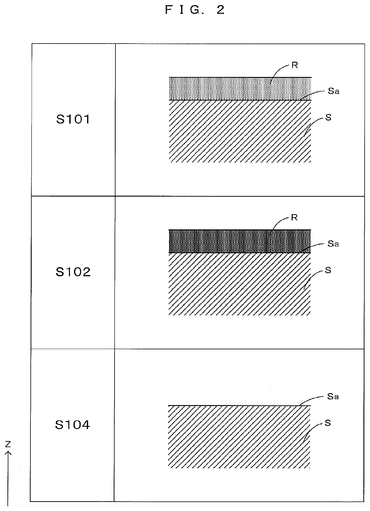
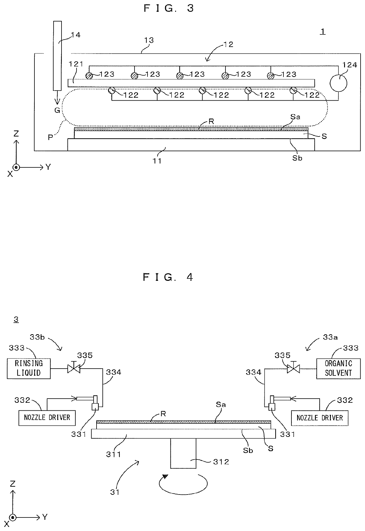
[0021]FIG. 1 is a flow chart showing an example of a substrate processing method according to the invention, FIG. 2 is a chart schematically showing an operation performed in FIG. 1, FIG. 3 is a diagram schematically showing an example of a plasma processing apparatus used in the substrate processing method of FIG. 1, and FIG. 4 is a diagram schematically showing an example of a processing liquid supply apparatus used in the substrate processing method of FIG. 1. An X direction, which is a horizontal direction, and a Y direction, which is a horizontal direction orthogonal to the X direction, or a Z direction, which is a vertical direction, are shown as appropriate in FIGS. 2 to 4.

[0022]In Step S101, a substrate S is loaded into a plasma processing apparatus 1. The substrate S has a front surface Sa and a back surface Sb opposite to the front surface Sa, and a resist film R is formed on the front surface Sa of the substrate S (FIGS. 2 and 3). Particularly, ions are implanted into a s...


PUM

PropertyMeasurementUnit
distanceaaaaaaaaaa
distanceaaaaaaaaaa
widthaaaaaaaaaa

Abstract

The radical supply step of supplying the radicals (active species) to the resist film R is performed in the plasma processing (Step S102). Then, the resist removal step of supplying the organic solvent having the low surface tension to the resist film R present on the front surface Sa of the substrate S after the radical supply step to remove the resist film R from the front surface Sa of the substrate S is performed (Step S104).

Description

CROSS REFERENCE TO RELATED APPLICATION[0001]The disclosure of Japanese Patent Application No.2020-052761 filed on Mar. 24, 2020 including specification, drawings and claims is incorporated herein by reference in its entirety.BACKGROUND OF THE INVENTION1. Field of the Invention[0002]This invention relates to a technique for performing a process to a substrate using a plasma and particularly to a technique for removing a resist film from a semiconductor substrate made of silicon or the like.2. Description of the Related Art[0003]Conventionally, a plasma ashing technique is one of methods for removing a resist film formed on a surface of a substrate. Plasma ashing is a technique for breaking carbon-hydrogen bonds in a resist film to remove the resist film or set the resist film in an easily removable state by causing ionic molecules and the like produced by a plasma to collide with the resist film formed on a substrate. In plasma ashing, a plasma generation space for generating a plasm...

Claims


Application Information

Patent Timeline
Patent Type & Authority Applications(United States)
IPC IPC(8): G03F7/36H01L21/02H01J37/32
CPCG03F7/36H01L21/02057H01J2237/327H01J37/3244H01J37/32715H01L21/31138H01L21/0206H01L21/67069H01L21/67051H01L21/31133H01L21/6708G03F7/427G03F7/422G03F7/42H01L21/67017H01L21/6715H01J37/32532
Inventor HORIKOSHI, AKIRANAKAMURA, SHOHEITAKATSUJI, SHIGERUKIMURA, TAKAHIRO
Owner DAINIPPON SCREEN MTG CO LTD
Why Eureka
Try Eureka