

Solid-state imaging device
a solid-state imaging and imaging element technology, applied in the direction of polarising elements, radioactive control devices, instruments, etc., can solve the problems of reducing the extinction ratio of the wire grid polarizer, reducing the transmittance, etc., to reduce the optical crosstalk, the long-term reliability of the imaging element may be deteriorated, and the corrosion resistance of metal materials or the lik
Active Publication Date: 2021-11-25
SONY SEMICON SOLUTIONS CORP
View PDF0 Cites 7 Cited by
- Summary
- Abstract
- Description
- Claims
- Application Information
AI Technical Summary
Benefits of technology
The patent text discusses how metal materials used in wire grid polarizers can become corrosive when exposed to outside air, leading to potential performance issues and reduced reliability. The text focuses on the use of certain materials and refractive indexes to prevent the formation of local batteries and abnormal precipitation of metal materials, which can impair the function of the wire grid polarizer and imaging element. By avoiding these materials and utilizing specific refractive indexes, the text proposes that the thickness of the imaging element can be reduced, resulting in reduced optical crosstalk, improved sensitivity, and no ripple effect.
Problems solved by technology
Further, as the value of nave increases, this leads to decrease of the transmittance and decrease of the extinction ratio of the wire grid polarizer.
Method used
View moreImage
Smart ImageViewing Examples

Examples
working example 1 (
2. Working example 1 (solid-state imaging devices of first to second aspects of present disclosure)
working example 2 (modification of working example 1)
3. Working example 2 (modification of working example 1)
working example 3 (another modification of working example 1)
4. Working example 3 (another modification of working example 1)
Login to View More PUM
| Property | Measurement | Unit |
|---|---|---|
| photoelectric | aaaaa | aaaaa |
| refractive index | aaaaa | aaaaa |
| and-space | aaaaa | aaaaa |
Abstract
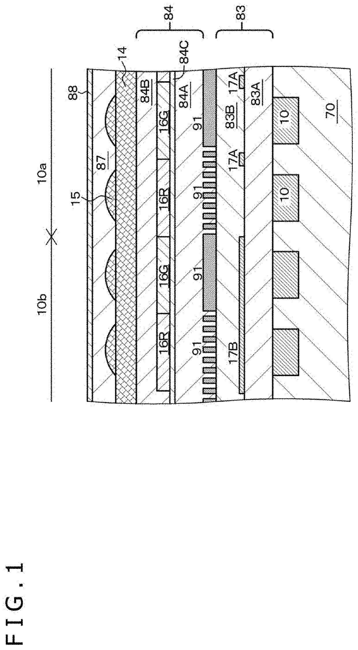
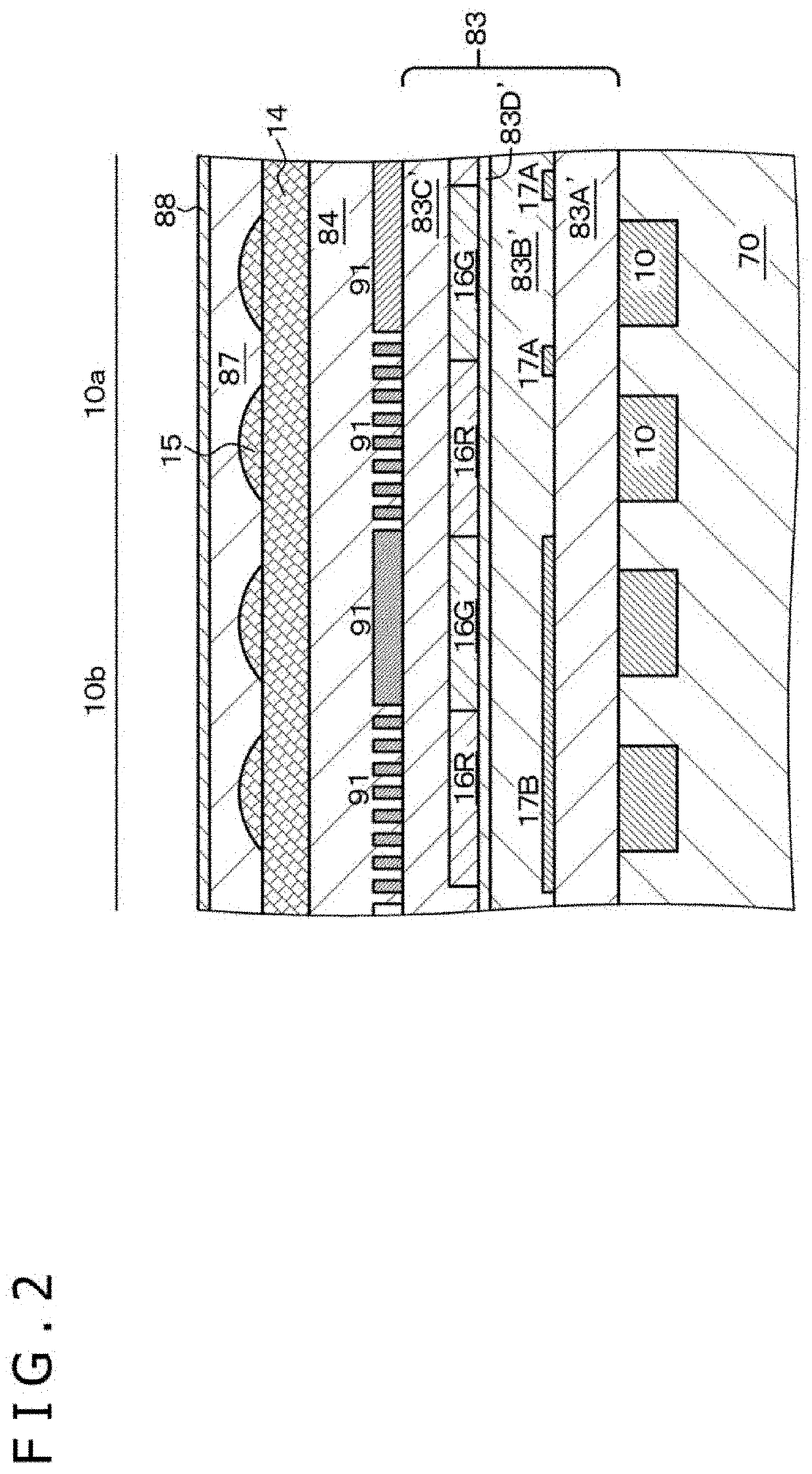
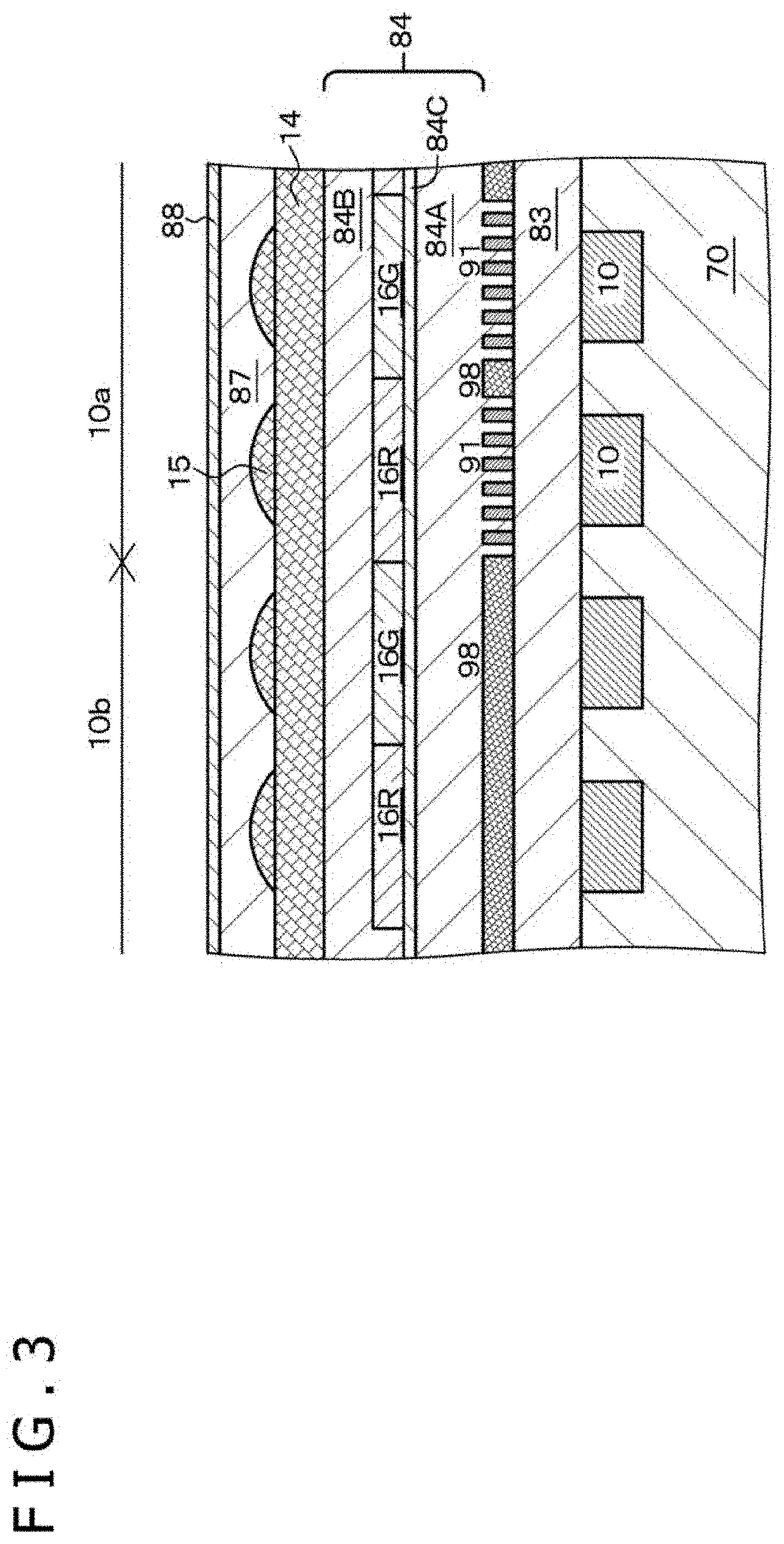
A solid-state imaging device includes an imaging element group in which imaging elements each having a photoelectric conversion portion 10 formed on or above a semiconductor substrate 70 and further having a wire grid polarizer 91 and an on-chip microlens 15 are arrayed in a two-dimensional matrix, and a first interlayer insulating layer 83 and a second interlayer insulating layer 84 provided on a light incident side of the photoelectric conversion portions 10. The wire grid polarizer 91 is provided between the first interlayer insulating layer 83 and the second interlayer insulating layer 84, and the on-chip microlens 15 is provided on the second interlayer insulating layer 84. The first interlayer insulating layer 83 and the second interlayer insulating layer 84 include an oxide material or a resin material, and the on-chip microlens includes SiN or SiON.
Description
TECHNICAL FIELD[0001]The present disclosure relates to a solid-state imaging device, and more particularly relates to a solid-state imaging device that includes a wire grid polarizer.BACKGROUND ART[0002]A solid-state imaging device that includes a plurality of imaging elements (photoelectric conversion elements) in which a wire grid polarizer (WGP) is provided is known, for example, from Japanese Patent Laid-Open No. 2016-164956. The imaging element includes, for example, a CCD element (Charge Coupled Device) or a CMOS (Complementary Metal Oxide Semiconductor) image sensor. The wire grid polarizer has a line-and-space structure. The direction in which the line-and-space structure extends is referred to as to “first direction” for the convenience of description, and the repetition direction of line portions (direction orthogonal to the first direction) is referred to as “second direction” for the convenience of description.[0003]As depicted in a conceptual diagram of FIG. 127, in the...
Claims
Login to View More Application Information
Patent Timeline
 Patent Type & AuthorityApplications(United States)
IPC IPC(8): H01L27/146G02B5/30H04N23/12
CPCH01L27/14612H01L27/14627H01L27/14643H01L27/14621H01L27/14623G02B5/3058H01L27/14629H01L27/14665H01L27/14638H01L27/1461H01L27/1464H01L27/14641H01L27/14605G02B3/0056G02B5/223
InventorYANAGITA, TAKESHIASATSUMA, TOMOHIKO
OwnerSONY SEMICON SOLUTIONS CORP